
Fab Transform AI Milestones
Fab Transform AI Milestones signifies a pivotal shift in the Silicon Wafer Engineering sector, encapsulating the integration of artificial intelligence into fabrication processes. This concept encompasses innovative practices that enhance operational efficiency and redefine strategic priorities for stakeholders, making it increasingly relevant in today's fast-evolving technological landscape. By leveraging AI-driven insights, companies can optimize their workflows, thus aligning with the broader narrative of digital transformation within the semiconductor domain.
As the Silicon Wafer Engineering ecosystem embraces these AI milestones, the implications are profound. Enhanced AI practices are reshaping competitive dynamics, fueling innovation cycles, and transforming stakeholder interactions. The integration of AI not only streamlines decision-making but also reorients long-term strategies towards more sustainable growth. Yet, this journey is not without its challenges; organizations must navigate adoption barriers, integration complexities, and evolving expectations to fully realize the transformative potential of AI.

Accelerate AI Integration for Fab Transform Milestones
Silicon Wafer Engineering companies should strategically invest in AI-focused partnerships and R&D initiatives to harness transformative capabilities in manufacturing processes. Implementing AI-driven solutions is expected to yield significant improvements in efficiency, cost reduction, and enhanced product quality, driving competitive advantage in the market.
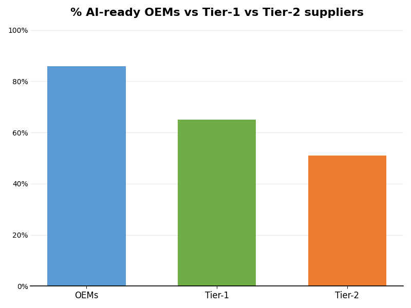
How AI is Revolutionizing Silicon Wafer Engineering?
AI Readiness Framework
The 6 Pillars of AI Readiness
Transformation Roadmap
Evaluate current AI capabilities and needs
Create a roadmap for AI integration
Deploy AI tools across engineering functions
Track and evaluate AI impact
Expand AI applications across the organization
Conduct a thorough assessment of existing AI tools and infrastructure, identifying gaps and opportunities for integration to enhance Silicon Wafer Engineering operations and achieve Fab Transform AI Milestones effectively.
Technology Partners
Formulate a comprehensive AI strategy , outlining specific goals, timelines, and resource allocation to optimize Silicon Wafer Engineering processes while ensuring alignment with broader organizational objectives and market trends.
Industry Standards
Execute the deployment of selected AI solutions tailored for Silicon Wafer Engineering , focusing on automation, predictive analytics, and quality control to enhance efficiency and mitigate operational risks effectively.
Internal R&D
Establish key performance indicators (KPIs) to monitor the effectiveness of AI implementations in real-time, enabling continuous improvement and adjustment of strategies to enhance Silicon Wafer Engineering outcomes and operational resilience.
Cloud Platform
Identify and scale successful AI practices from initial implementations, promoting knowledge sharing and collaboration across departments to maximize the benefits and integrate AI-driven efficiencies in Silicon Wafer Engineering .
Technology Partners
AI is dramatically transforming the semiconductor industry by automating chip design and verification with EDA tools like DSO.ai, reducing 5nm chip design timelines from months to weeks.
– Aart de Geus, Co-CEO and Founder of Synopsys
Compliance Case Studies


Seize the opportunity to revolutionize your silicon wafer engineering with AI . Transform challenges into competitive advantages and lead the industry in innovation today.
Take TestRisk Senarios & Mitigation
Neglecting Compliance Regulations
Legal repercussions arise; ensure regular audits.
Ignoring Data Security Measures
Data breaches occur; implement robust encryption protocols.
Overlooking Algorithmic Bias
Unfair outcomes result; conduct thorough bias assessments.
Experiencing Operational Failures
Production delays happen; establish contingency plans.
Assess how well your AI initiatives align with your business goals
Glossary
Work with Atomic Loops to architect your AI implementation roadmap — from PoC to enterprise scale.
Contact NowFrequently Asked Questions
- Fab Transform AI Milestones enhances operational efficiency through AI-driven automation and smart workflows.
- It improves product quality by minimizing human errors and ensuring consistent process control.
- Organizations can leverage real-time data analytics for informed decision-making and rapid adjustments.
- This technology fosters innovation by accelerating product development cycles and reducing time to market.
- Companies gain a competitive edge through improved performance and customer satisfaction metrics.
- Begin with a clear assessment of your current processes and identify improvement areas.
- Formulate a strategic roadmap that outlines specific goals and expected outcomes for AI integration.
- Engage with stakeholders early to ensure buy-in and collaborative efforts throughout the process.
- Pilot projects can help in testing AI applications before full-scale implementation.
- Invest in training and upskilling your workforce to effectively use new AI technologies.
- AI adoption leads to significant cost savings by automating repetitive and time-consuming tasks.
- Companies often experience enhanced quality control, resulting in fewer defects and reworks.
- AI can optimize resource allocation, maximizing production efficiency and throughput rates.
- Business agility improves, enabling faster responses to market demands and technological advancements.
- Enhanced data insights from AI facilitate better forecasting and strategic planning initiatives.
- Resistance to change from employees can hinder the adoption of new technologies and processes.
- Data quality issues must be addressed to ensure effective AI model training and performance.
- Integration with legacy systems may pose technical hurdles that require careful planning.
- Skill gaps in the workforce can limit the effective implementation and utilization of AI tools.
- Establishing robust security measures is critical to protect sensitive data during AI integration.
- Organizations should consider implementing AI when they have a clear understanding of their business goals.
- A readiness assessment of existing technology infrastructure can indicate preparedness for AI adoption.
- Market pressures and competitive landscape changes may necessitate timely AI integration.
- Companies experiencing declining efficiency or increasing operational costs should prioritize AI solutions.
- Aligning AI implementation with upcoming product launches can maximize its impact and effectiveness.
- Compliance with industry standards is essential to ensure safety and reliability in AI applications.
- Organizations must stay informed about evolving regulations concerning data privacy and security.
- Documentation and transparency in AI decision-making processes help maintain regulatory compliance.
- Engaging with regulatory bodies early can facilitate smoother approvals for AI projects.
- Establishing a governance framework ensures adherence to compliance requirements throughout implementation.
- Predictive maintenance powered by AI minimizes equipment downtime and enhances productivity.
- AI-driven quality assurance systems detect defects earlier in the production process.
- Real-time process monitoring using AI optimizes manufacturing conditions for better yields.
- Supply chain optimization through AI enhances inventory management and reduces waste.
- AI applications in design simulation expedite the development of new wafer technologies.
- Define clear KPIs aligned with your business objectives to evaluate AI performance effectively.
- Regularly track and analyze production metrics to assess improvements post-AI implementation.
- Employee feedback can provide insights into the practical impact of AI on workflows.
- Cost savings and ROI calculations should be monitored to ensure financial viability of AI projects.
- Continuous improvement cycles allow organizations to refine AI applications based on measured outcomes.