
Future Visionary AI Silicon Fusion
In the realm of Silicon Wafer Engineering, "Future Visionary AI Silicon Fusion " represents a pivotal convergence of artificial intelligence and semiconductor technology. This concept encapsulates the integration of advanced AI methodologies into wafer production and design, aiming to enhance operational efficiencies and innovation. As stakeholders navigate an evolving landscape, embracing this transformative approach is essential for aligning with the strategic priorities dictated by rapid technological advancements.
The ecosystem surrounding Silicon Wafer Engineering is increasingly influenced by AI-driven practices that redefine competitive dynamics and innovation cycles. As organizations adopt these AI solutions, they are witnessing enhanced efficiency and informed decision-making, which collectively steer long-term strategic direction. While the potential for growth is substantial, challenges such as adoption barriers , integration complexities, and shifting stakeholder expectations must be navigated effectively to harness the full benefits of this fusion.

Transform Your Operations with AI-Driven Strategies
Silicon Wafer Engineering firms should strategically invest in partnerships that leverage AI technologies to enhance manufacturing processes and predictive analytics. Implementing these AI-driven solutions is expected to yield significant operational efficiencies, reduced costs, and a strong competitive advantage in a rapidly evolving market.
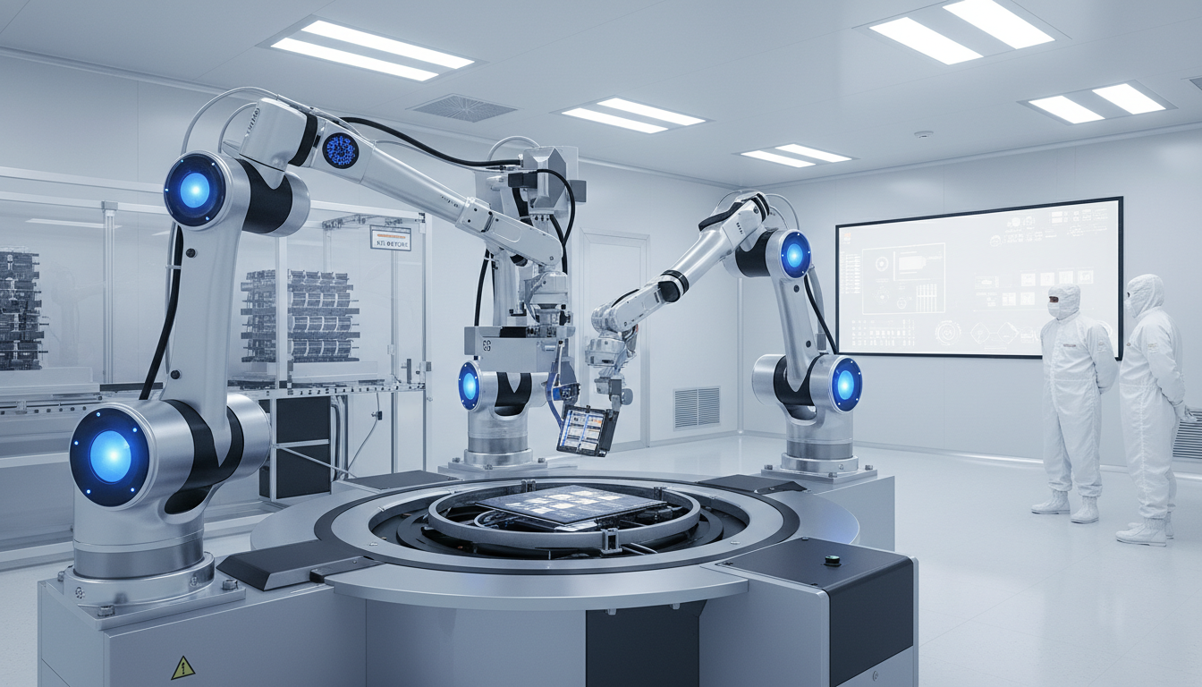
How AI is Shaping the Future of Silicon Wafer Engineering?
AI is dramatically transforming the semiconductor industry, especially in chip design, with AI-powered EDA tools automating repetitive tasks like schematic generation and layout optimization to accelerate development.
– TSMC Executive Team, Taiwan Semiconductor Manufacturing CompanyCompliance Case Studies
Transform your Silicon Wafer Engineering with AI-driven solutions. Seize the competitive edge and redefine your operational excellence today—don't let industry advancements pass you by.
Take TestRisk Senarios & Mitigation
Ignoring Compliance Regulations
Legal issues arise; ensure regular compliance audits.
Data Security Breaches
Sensitive data exposed; employ robust encryption methods.
AI Bias in Decision Making
Unfair outcomes occur; implement diverse training datasets.
Operational Downtime Risks
Production halts; create a comprehensive backup plan.
Assess how well your AI initiatives align with your business goals
Glossary
Work with Atomic Loops to architect your AI implementation roadmap — from PoC to enterprise scale.
Contact NowFrequently Asked Questions
- Future Visionary AI Silicon Fusion enhances silicon wafer production through AI-driven automation.
- It optimizes manufacturing processes, resulting in reduced waste and increased yield.
- The approach fosters innovation by enabling rapid prototyping and design iterations.
- It allows for real-time monitoring and analytics, improving decision-making capabilities.
- Companies can achieve higher quality standards and faster market entry with this technology.
- Begin by assessing your current infrastructure to identify integration points for AI.
- Engage stakeholders to ensure alignment on objectives and resource allocation.
- Develop a phased implementation plan that includes pilot projects for testing.
- Invest in training and upskilling your workforce to leverage AI tools effectively.
- Monitor progress and gather feedback to refine the implementation strategy continuously.
- AI enhances productivity by automating routine tasks and optimizing workflows.
- Companies benefit from improved defect detection rates, minimizing costly errors.
- Data-driven insights from AI lead to better resource management and cost savings.
- Faster innovation cycles result in a competitive edge in product offerings.
- Overall, organizations can expect a significant return on investment through AI integration.
- Common challenges include data quality issues and integration complexities with legacy systems.
- Change management can be difficult as employees may resist new technologies.
- Compliance with industry regulations requires careful planning and execution.
- Identifying the right AI tools and solutions is crucial for successful adoption.
- Establishing a clear strategy to address these challenges minimizes implementation risks.
- Evaluate your organization's readiness by assessing current technological capabilities.
- Market conditions and competitive pressures can indicate urgency for adoption.
- A clear strategic vision should guide the timing of AI integration initiatives.
- Pilot projects can help gauge effectiveness before full-scale implementation.
- Consider ongoing technological advancements to stay ahead in the industry.
- AI can optimize the design of wafers, improving performance and efficiency.
- Predictive maintenance using AI reduces downtime and extends equipment lifespan.
- Quality control processes benefit from AI through enhanced defect analysis.
- Supply chain optimization is achievable with AI's data analysis capabilities.
- Customization of wafer production processes can be enhanced through AI-driven insights.
- Investing now allows for early adoption advantages in a rapidly evolving market.
- AI can significantly reduce operational costs and improve profit margins.
- The technology fosters innovation, enabling faster response to market demands.
- Competitive advantages can be gained through improved product quality and efficiency.
- Long-term sustainability and growth can be achieved by leveraging AI capabilities.