Fab AI Future Workforce
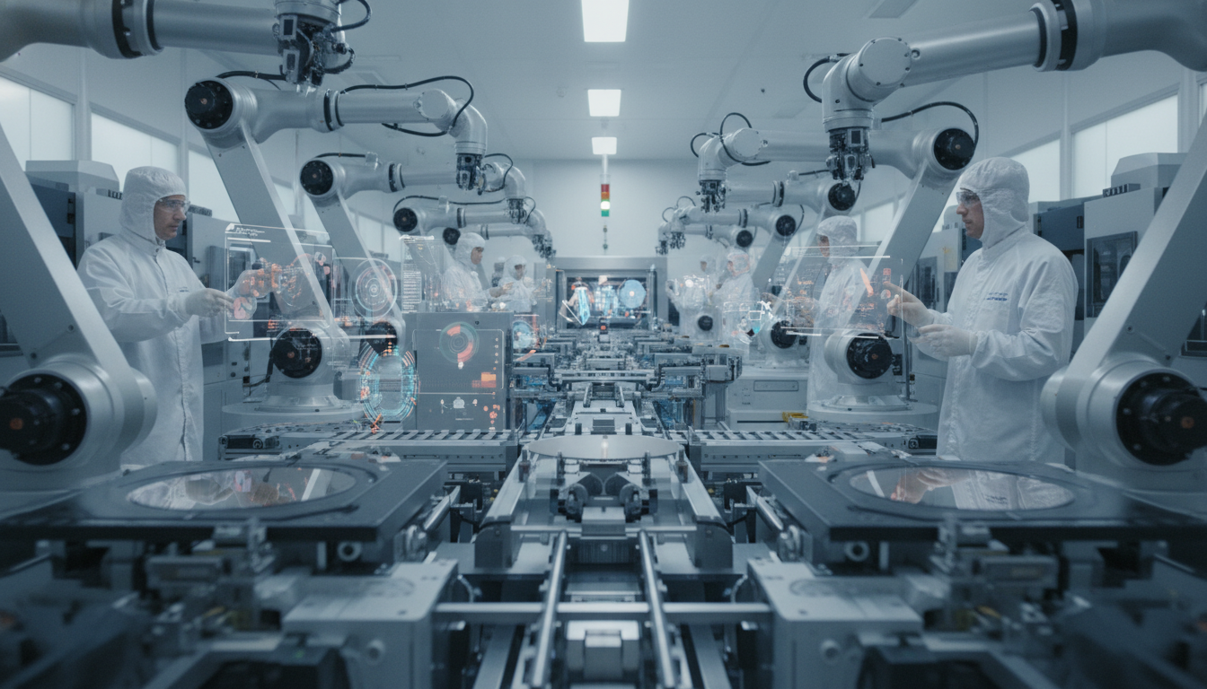
The " Fab AI Future Workforce " represents a transformative shift in the Silicon Wafer Engineering sector, where artificial intelligence is integrated into fabrication processes and workforce strategies. This concept emphasizes the fusion of advanced AI technologies with skilled labor to enhance productivity, innovation, and operational efficiency. As the industry evolves, it becomes crucial for stakeholders to understand how this synergy not only streamlines manufacturing but also aligns with broader trends in digital transformation and automation.
In the Silicon Wafer Engineering ecosystem, the integration of AI practices is redefining competitive landscapes and innovation cycles. Stakeholders are witnessing a profound impact on decision-making processes and operational dynamics, leading to greater efficiency and agility . However, while the potential for growth and enhanced stakeholder value is significant, challenges such as adoption barriers , integration complexities, and shifting expectations must be navigated thoughtfully. As the industry embraces AI, it opens new avenues for innovation while demanding a strategic approach to workforce development and technology integration.

Leverage AI Strategies for a Competitive Edge in Silicon Wafer Engineering
Companies in the Silicon Wafer Engineering industry should strategically invest in AI-driven solutions and forge partnerships with innovative tech firms to enhance workforce capabilities. By implementing these AI strategies, businesses can achieve greater operational efficiencies, improved product quality, and a strong competitive advantage in the market.
How is AI Shaping the Future of Silicon Wafer Engineering?
We are going to have to build magnificent factories for chips and AI supercomputers, requiring hundreds of thousands, maybe millions, of skilled craftspeople like plumbers, electricians, and technicians to support the AI revolution in semiconductor manufacturing.
– Jensen Huang, CEO of NVIDIACompliance Case Studies


Embrace AI-driven solutions to enhance productivity and innovation in Silicon Wafer Engineering . Stay ahead of the curve and transform your business today!
Take TestRisk Senarios & Mitigation
Ignoring Data Privacy Regulations
Legal penalties result; enforce data handling policies.
Underestimating AI Bias Impact
Decision-making errors occur; train on diverse datasets.
Overlooking Cybersecurity Threats
Data breaches happen; implement robust security measures.
Neglecting Workforce Training Needs
Operational inefficiencies arise; invest in continuous education.
Assess how well your AI initiatives align with your business goals
Glossary
Work with Atomic Loops to architect your AI implementation roadmap — from PoC to enterprise scale.
Contact NowFrequently Asked Questions
- The Fab AI Future Workforce leverages AI to optimize manufacturing processes effectively.
- It enhances operational efficiency by automating repetitive tasks within the workflow.
- This technology facilitates data-driven decision-making through real-time analytics.
- Companies can achieve significant cost reductions while improving product quality.
- Ultimately, it positions organizations to remain competitive in a rapidly evolving market.
- Begin with a clear assessment of your current processes and objectives.
- Identify specific areas where AI can add measurable value and efficiency.
- Allocate resources for training and change management to ensure smooth transitions.
- Pilot programs can help validate AI applications before full-scale implementation.
- Engage stakeholders early to foster buy-in and facilitate successful integration.
- AI adoption can lead to improved efficiency and reduced operational costs significantly.
- Companies often see enhanced product quality and reduced defect rates over time.
- AI-driven insights allow for better forecasting and resource allocation decisions.
- Enhanced agility enables quicker responses to market demands and changes.
- Overall, organizations gain a competitive edge in innovation and service delivery.
- Common challenges include resistance to change from employees and stakeholders.
- Data quality and accessibility can hinder successful AI implementation efforts.
- Integration with existing systems may require additional investment and time.
- Skill gaps in the workforce necessitate ongoing training and development programs.
- A clear strategy for risk management is essential to navigate potential setbacks.
- Evaluate your organization’s digital maturity and readiness for technological shifts.
- Market demand changes can signal the need for AI-driven efficiencies and improvements.
- Consider upcoming product launches as opportunities to integrate AI solutions.
- Timing should align with strategic goals to ensure maximum impact and value.
- Regular assessments can help identify optimal windows for AI implementation.
- Ensure compliance with industry-specific regulations that govern data usage and privacy.
- Understand intellectual property laws related to AI technologies and innovations.
- Stay informed about evolving standards in semiconductor manufacturing practices.
- Engage with legal experts to navigate complex regulatory landscapes effectively.
- Maintain transparency in AI applications to build trust with customers and stakeholders.
- Establish clear metrics and KPIs relevant to your business objectives upfront.
- Track improvements in productivity, quality, and cost reductions over time.
- Conduct regular reviews to assess the impact of AI on operational efficiency.
- Benchmark against industry standards to understand competitive positioning.
- Use qualitative feedback from teams to gauge satisfaction and performance improvements.