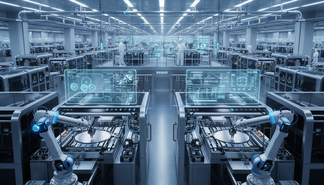
AI Future Space Analog Fab
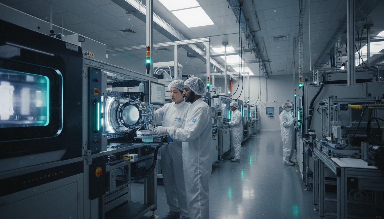
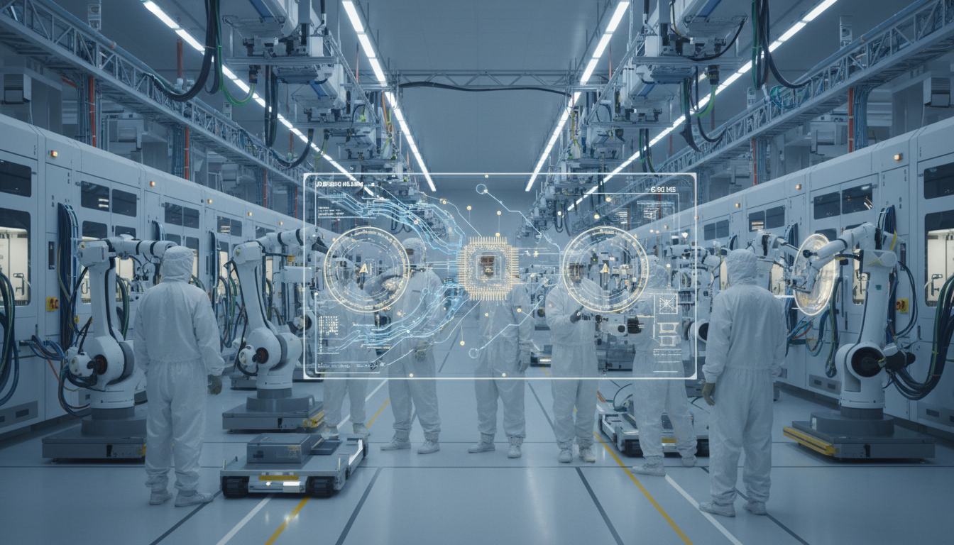
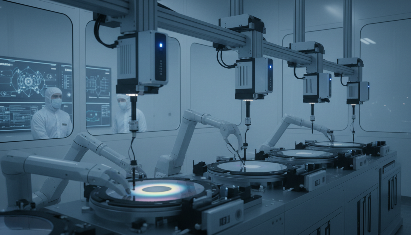
The "AI Future Space Analog Fab" represents a transformative approach within the Silicon Wafer Engineering sector, integrating artificial intelligence to enhance fabrication processes. This concept encompasses the utilization of AI algorithms and data analytics to drive innovation and operational efficiency in creating silicon wafer s. As stakeholders navigate an increasingly complex landscape, the relevance of AI in this context has become paramount, aligning with the industry's pivot towards digital transformation and smart manufacturing practices.
The ecosystem surrounding Silicon Wafer Engineering is rapidly evolving due to the integration of AI-driven methodologies, which are reshaping competitive dynamics and fostering new avenues for innovation. By leveraging advanced AI technologies, organizations can enhance decision-making, streamline production processes, and improve stakeholder interactions. However, while the potential for growth is substantial, challenges such as adoption barriers and the complexity of integration must be addressed to fully realize the advantages of these transformative practices.

Harness AI Innovations for Silicon Wafer Engineering
Companies in the Silicon Wafer Engineering sector should strategically invest in AI Future Space Analog Fab initiatives and form partnerships with leading AI technology firms to enhance their operational capabilities. Implementing AI-driven solutions will yield significant benefits such as improved manufacturing efficiency, higher product quality, and a stronger competitive edge in the market.
How AI is Revolutionizing Silicon Wafer Engineering?
We manufactured the most advanced AI chips in the world, in the most advanced fab in the world, here in America for the first time, marking the beginning of a new AI industrial revolution.
– Jensen Huang, CEO of NVIDIACompliance Case Studies

Seize the opportunity to lead the Silicon Wafer Engineering industry. Transform your operations with state-of-the-art AI solutions and outpace your competition today.
Take TestRisk Senarios & Mitigation
Neglecting Regulatory Compliance Standards
Legal penalties arise; conduct regular compliance audits.
Compromising Data Security Measures
Data breaches occur; implement advanced encryption protocols.
Overlooking Algorithmic Bias Issues
Unfair outcomes result; establish diverse training data sets.
Experiencing System Operational Failures
Downtime affects productivity; reinforce backup and recovery systems.
Assess how well your AI initiatives align with your business goals
Glossary
Work with Atomic Loops to architect your AI implementation roadmap — from PoC to enterprise scale.
Contact NowFrequently Asked Questions
- AI Future Space Analog Fab integrates advanced AI technologies into silicon wafer manufacturing processes.
- This technology enhances precision and reduces production errors significantly in wafer fabrication.
- It enables real-time monitoring and predictive maintenance for improved operational efficiency.
- Companies benefit from faster turnaround times and reduced costs through automation.
- Overall, it drives innovation and competitiveness in the Silicon Wafer Engineering sector.
- Start by assessing current workflows and identifying areas for AI integration.
- Engage cross-functional teams to ensure alignment with business objectives and goals.
- Pilot projects can be initiated to validate AI applications before full-scale deployment.
- Consider leveraging partnerships with AI specialists to facilitate knowledge transfer.
- Allocate resources for training and change management to support smooth implementation.
- Organizations can achieve improved yield rates due to enhanced process control and monitoring.
- AI implementations lead to significant reductions in production costs and time.
- Companies experience increased customer satisfaction through faster delivery and quality improvements.
- Data-driven insights enable better decision-making and strategic planning.
- Enhanced competitiveness results from the ability to innovate rapidly in response to market demands.
- Resistance to change among employees can hinder the adoption of new technologies.
- Integrating AI with legacy systems may pose technical challenges and require additional resources.
- Data privacy and security concerns must be addressed to ensure compliance with regulations.
- Skill gaps in the workforce necessitate training and upskilling to effectively use AI tools.
- Developing a clear strategy and roadmap can mitigate risks associated with implementation.
- Organizations should consider adopting AI when facing increasing production demands and complexity.
- If existing processes show inefficiencies, it's an optimal time to explore AI technologies.
- Market competition may drive the need for AI to maintain or improve market position.
- Emerging technologies and industry trends can signal readiness for AI adoption.
- Strategic planning should align AI implementation with long-term business goals and objectives.
- Compliance with industry standards is crucial for adopting AI technologies in manufacturing.
- Data handling and privacy regulations should be prioritized during implementation.
- Organizations must ensure transparency in AI algorithms to maintain stakeholder trust.
- Regular audits and assessments can help companies remain compliant with evolving regulations.
- Collaboration with regulatory bodies can provide guidance on best practices in AI deployment.
- Establish clear objectives and performance metrics to measure AI effectiveness early on.
- Involve stakeholders at all levels to foster a culture of innovation and collaboration.
- Regularly review and refine AI strategies based on performance and feedback from users.
- Invest in continuous training and development to keep the workforce updated on AI advancements.
- Utilize a phased implementation approach to manage risks and demonstrate quick wins effectively.