
AI Fab Vision Decent Auton
AI Fab Vision Decent Auton represents a paradigm shift within the Silicon Wafer Engineering sector, integrating advanced artificial intelligence to optimize manufacturing processes and enhance operational efficiency. This concept encapsulates the use of AI technologies to automate and refine fabrication activities, making them more responsive to real-time data and market demands. As stakeholders increasingly prioritize innovation and agility, the relevance of AI Fab Vision Decent Auton becomes paramount for those striving to remain competitive in a rapidly evolving landscape.
The Silicon Wafer Engineering ecosystem is witnessing a transformative wave driven by AI implementation, fundamentally altering competitive dynamics and fostering new innovation cycles. AI-driven practices not only enhance decision-making but also streamline operations, enabling stakeholders to adapt swiftly to changing conditions. While the potential for efficiency gains and strategic advancements is significant, challenges such as integration complexity and shifting expectations must be addressed. Growth opportunities abound for organizations that can navigate these hurdles, positioning themselves at the forefront of technological evolution within their domain.

Accelerate AI Integration in Silicon Wafer Engineering
Silicon Wafer Engineering firms should strategically invest in AI Fab Vision Decent Auton technologies and forge partnerships with leading AI innovators to enhance their operational capabilities. The implementation of these AI solutions is expected to drive significant efficiencies, reduce costs, and create a competitive edge in the rapidly evolving market.
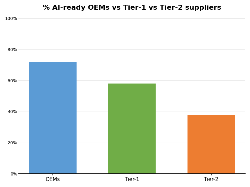
How AI is Revolutionizing Silicon Wafer Engineering?
We're not building chips anymore, those were the good old days. We are an AI factory now. A factory helps customers make money.
– Jensen Huang, CEO of NVIDIACompliance Case Studies


Seize the opportunity to revolutionize your Silicon Wafer Engineering processes. Leverage AI-driven solutions for unparalleled efficiency and market leadership. Time to act is now!
Take TestRisk Senarios & Mitigation
Ignoring Data Privacy Regulations
Data breaches risk; enforce robust data management policies.
Overlooking AI Model Bias
Unfair outcomes arise; ensure diverse training data sets.
Failing Cybersecurity Measures
Increased vulnerability; implement strong security protocols.
Neglecting Compliance Standards
Legal penalties loom; conduct regular compliance audits.
Assess how well your AI initiatives align with your business goals
Glossary
Work with Atomic Loops to architect your AI implementation roadmap — from PoC to enterprise scale.
Contact NowFrequently Asked Questions
- AI Fab Vision Decent Auton automates processes in Silicon Wafer Engineering for efficiency.
- It leverages machine learning algorithms to enhance precision in manufacturing.
- The solution minimizes human error through intelligent data analysis and validation.
- Companies benefit from improved throughput and reduced cycle times in production.
- Overall, it fosters innovation by enabling faster product development cycles.
- Start with a clear assessment of your current processes and systems.
- Identify specific use cases where AI can deliver immediate value and impact.
- Engage stakeholders across departments to ensure alignment and support.
- Begin with pilot projects to test AI capabilities in a controlled environment.
- Gradually scale up based on pilot results and strategic objectives for implementation.
- Adopting AI can lead to significant cost savings through optimized operations.
- Faster decision-making is facilitated by real-time data analytics and insights.
- Improved quality control results from enhanced monitoring and predictive maintenance.
- AI-driven innovations can provide a competitive edge in technology advancements.
- Overall, ROI improves as efficiency and productivity levels are elevated.
- Common challenges include integration with legacy systems and data silos.
- Staff resistance to change can hinder the successful adoption of new technologies.
- Ensuring data quality and availability is crucial for effective AI implementation.
- Regulatory compliance may pose additional hurdles in certain applications.
- Developing a robust change management strategy is essential for overcoming obstacles.
- The right time is when you have a clear business case for AI implementation.
- Assess your organization's readiness for digital transformation and cultural change.
- Market pressures may necessitate faster adoption to remain competitive.
- Identify technological advancements that align with your strategic goals.
- Regularly review industry trends to gauge the urgency for AI adoption.
- Prioritize stakeholder engagement to secure buy-in and collaborative efforts.
- Establish clear metrics to evaluate the success of AI initiatives.
- Keep a focus on continuous training and upskilling of your workforce.
- Iterate and improve based on feedback and data insights throughout the process.
- Maintain flexibility to adapt strategies as technology and market needs evolve.