
AI Fab Vision Ambient Intel
AI Fab Vision Ambient Intel represents a transformative approach within the Silicon Wafer Engineering sector, integrating advanced artificial intelligence to enhance operational efficiency and decision-making. This concept encompasses the use of AI technologies to create an interconnected environment that optimizes processes and fosters innovation. For industry stakeholders, understanding this paradigm is crucial as it aligns with the ongoing AI-led transformation, reflecting shifting operational priorities that are increasingly data-driven and technology-focused.
The Silicon Wafer Engineering ecosystem is undergoing significant changes due to the influence of AI Fab Vision Ambient Intel. As AI-driven practices gain traction, competitive dynamics are evolving, leading to faster innovation cycles and deeper stakeholder engagement. These advancements not only enhance operational efficiency but also refine strategic decision-making processes. However, the journey towards full AI integration presents challenges such as adoption barriers and the complexity of seamless technology integration. Recognizing these hurdles alongside the potential for growth opportunities is essential for navigating the future landscape of the sector.

Empower Your Silicon Wafer Engineering with AI-Driven Strategies
Companies in the Silicon Wafer Engineering industry should strategically invest in AI Fab Vision Ambient Intel partnerships and collaborative research initiatives. By implementing AI technologies, businesses can expect significant improvements in operational efficiency, market responsiveness, and a sustainable competitive edge .
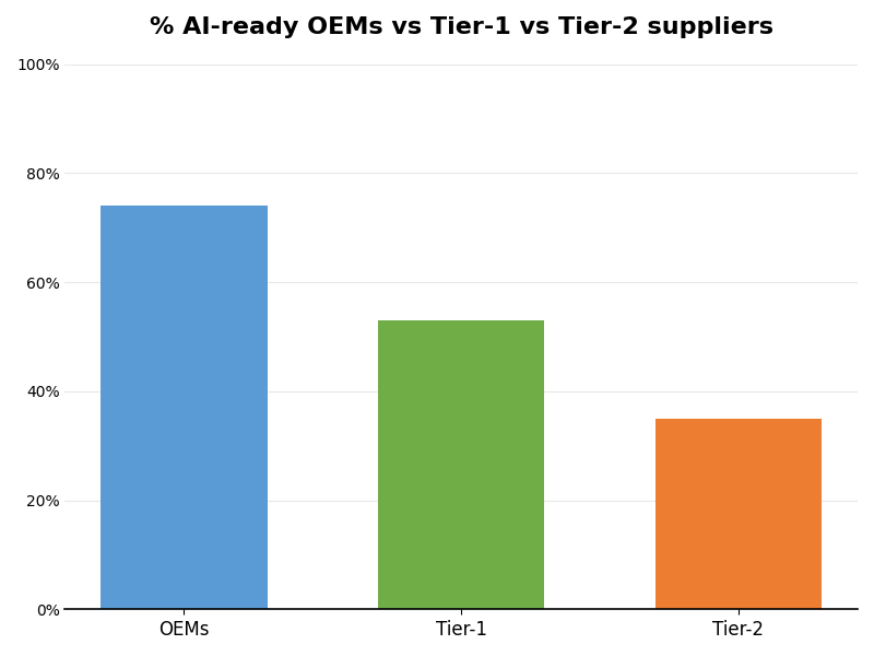
How AI is Transforming Silicon Wafer Engineering?
We're not building chips anymore, those were the good old days. We are an AI factory now. A factory helps customers make money.
– Jensen Huang, CEO of NVIDIACompliance Case Studies


Unlock the power of AI-driven solutions to elevate your operations and outpace competitors. Transform challenges into opportunities and lead the market with confidence.
Take TestRisk Senarios & Mitigation
Failing ISO Compliance Standards
Legal penalties arise; maintain regular audits.
Ignoring Data Privacy Protocols
Data breaches occur; enforce strict access controls.
Overlooking AI Bias Issues
Skewed results emerge; conduct regular bias assessments.
Experiencing Operational Failures
Production delays happen; establish robust failover systems.
Assess how well your AI initiatives align with your business goals
Glossary
Work with Atomic Loops to architect your AI implementation roadmap — from PoC to enterprise scale.
Contact NowFrequently Asked Questions
- AI Fab Vision Ambient Intel enhances manufacturing processes through intelligent automation strategies.
- It provides real-time monitoring and data analytics to improve decision-making efficiency.
- The system integrates seamlessly with existing processes to minimize disruptions and downtime.
- Organizations benefit from optimized resource allocation and reduced operational costs.
- This technology fosters innovation by enabling faster response to market changes.
- Start by assessing your current systems and identifying areas for AI integration.
- Develop a clear roadmap that outlines objectives, timelines, and resource allocations.
- Engage stakeholders early to ensure buy-in and support for the AI initiative.
- Consider initiating a pilot program to test AI capabilities on a smaller scale.
- Leverage partnerships with AI vendors to facilitate smoother implementation processes.
- AI can significantly enhance production efficiency, leading to lower operational costs.
- Companies often experience improved yield rates and product quality through precise monitoring.
- Data-driven insights enable faster decision-making, enhancing competitiveness in the market.
- AI solutions can improve customer satisfaction by reducing lead times and errors.
- Return on investment manifests through streamlined workflows and reduced resource wastage.
- Common obstacles include data silos and lack of integration with existing systems.
- Workforce resistance is typical; effective change management strategies are crucial.
- Budget constraints may limit initial investments in AI technologies and training.
- Ensuring data quality and relevance is vital for successful AI outcomes.
- Mitigation strategies include phased rollouts and continuous stakeholder engagement.
- The ideal time is when your facility experiences inefficiencies or high operational costs.
- Market competition can also signal the need for AI integration to maintain leadership.
- If there’s an increasing volume of data, AI can help leverage this information effectively.
- Consider adopting AI when resources allow for necessary training and infrastructure upgrades.
- Regular assessments of technology trends can inform timely adoption of AI solutions.
- Compliance with industry standards is essential to ensure AI deployment is lawful.
- Data privacy regulations must be adhered to, especially with customer information.
- Understand environmental regulations that may impact AI technologies in manufacturing.
- Regular audits and assessments can help maintain compliance throughout the AI lifecycle.
- Staying updated on regulatory changes is crucial for long-term AI sustainability.
- Begin with a clear strategy that aligns AI initiatives with business goals and objectives.
- Involve cross-functional teams to foster collaboration and a shared vision for AI.
- Invest in training programs to equip staff with necessary AI skills and knowledge.
- Focus on continuous monitoring and evaluation to refine AI implementations over time.
- Establish metrics to measure success and inform future AI investments and strategies.