AI 2030 Hyper Eff Wafer Fab
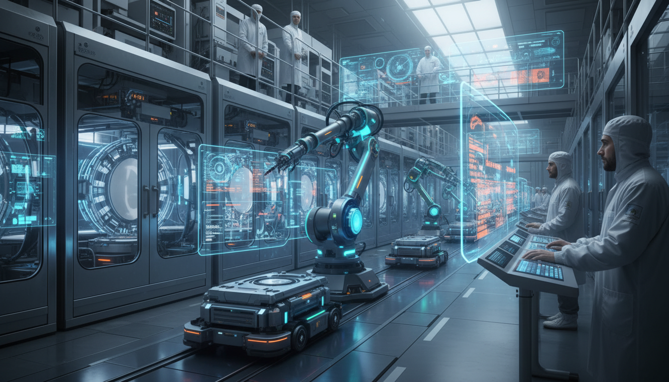
The concept of " AI 2030 Hyper Eff Wafer Fab " represents a transformative vision within the Silicon Wafer Engineering sector, where artificial intelligence is harnessed to enhance fabrication processes. This initiative focuses on optimizing efficiency and precision across wafer production , emphasizing the integration of intelligent systems that streamline operations. As industry stakeholders navigate an increasingly competitive landscape, aligning with this concept becomes crucial for maintaining relevance and fostering innovation in their strategic priorities.
The Silicon Wafer Engineering ecosystem is significantly impacted by AI-driven methodologies, leading to a redefinition of competitive dynamics and innovation cycles. These advanced practices enhance operational efficiency and decision-making processes, empowering stakeholders to adapt to evolving market conditions with agility . However, while growth opportunities abound, challenges such as adoption barriers and integration complexity must be acknowledged. The ability to meet changing expectations will ultimately determine the success of organizations embracing this AI-led transformation.

Drive Strategic AI Adoption for 2030 Wafer Fab Excellence
Silicon Wafer Engineering companies must prioritize strategic investments and forge partnerships centered on AI technologies to enhance wafer fabrication processes. By implementing AI solutions, firms can expect significant improvements in operational efficiency, cost reductions, and a stronger competitive edge in the marketplace.
How is AI Transforming Silicon Wafer Fabrication by 2030?
We are an AI factory now, shifting from traditional chip building to enabling hyper-efficient AI production that will power wafer fabrication and semiconductor advancements by 2030.
– Jensen Huang, CEO of Nvidia Corp.Compliance Case Studies


Leverage AI-driven solutions to transform your Silicon Wafer Engineering processes. Stay ahead of competitors and unlock groundbreaking efficiencies today!
Take TestRisk Senarios & Mitigation
Ignoring Compliance Regulations
Legal repercussions arise; establish regular audits.
Data Security Breaches Occur
Sensitive data compromised; enhance encryption protocols.
AI Decision-Making Bias
Inaccurate outputs emerge; implement diverse training data.
Operational System Failures
Production delays happen; conduct routine system checks.
Assess how well your AI initiatives align with your business goals
Glossary
Work with Atomic Loops to architect your AI implementation roadmap — from PoC to enterprise scale.
Contact NowFrequently Asked Questions
- AI 2030 Hyper Eff Wafer Fab integrates AI for enhanced manufacturing efficiency.
- It optimizes production processes, reducing waste and improving yield significantly.
- The framework enables real-time monitoring and predictive maintenance for equipment.
- Companies benefit from advanced analytics that drive informed decision-making.
- This approach positions businesses competitively in a rapidly evolving market.
- Start by assessing your current systems and identifying potential AI applications.
- Develop a clear strategy that aligns with your business objectives and resources.
- Engage stakeholders to ensure buy-in and facilitate a smooth transition.
- Consider pilot projects to test AI solutions before full-scale implementation.
- Continuous training and support for your team are crucial for successful adoption.
- AI implementation typically leads to reduced operational costs and enhanced productivity.
- Companies can expect improved product quality through better defect detection.
- Faster innovation cycles allow for quicker responses to market demands.
- Data-driven insights lead to more effective resource allocation and planning.
- The competitive edge gained can significantly enhance market positioning.
- Common challenges include resistance to change among staff and stakeholders.
- Data quality and availability can hinder AI model effectiveness.
- Integration with legacy systems often presents technical obstacles.
- Compliance with industry regulations necessitates careful planning and implementation.
- Developing a robust training program is essential to mitigate knowledge gaps.
- The ideal time is when your organization is ready for digital transformation.
- Market demands for efficiency and quality are increasing rapidly.
- A strong foundation in data management facilitates smoother AI adoption.
- Evaluating competitors’ progress can provide insights into timing.
- Regularly reviewing technological advancements can help identify opportunities.
- Applications include predictive maintenance and automated quality control processes.
- AI can enhance supply chain management and inventory forecasting accuracy.
- Real-time data analytics streamline decision-making in production environments.
- Customized solutions can address specific challenges unique to wafer fabrication.
- Compliance monitoring becomes more efficient with AI-driven insights and reporting.
- Investing in AI can lead to substantial long-term cost savings and efficiency gains.
- It positions your company as a leader in technological innovation within the industry.
- AI enhances customer satisfaction through improved product quality and reliability.
- The ability to analyze data effectively can unlock new business opportunities.
- Ultimately, staying competitive in a fast-evolving market requires such investments.