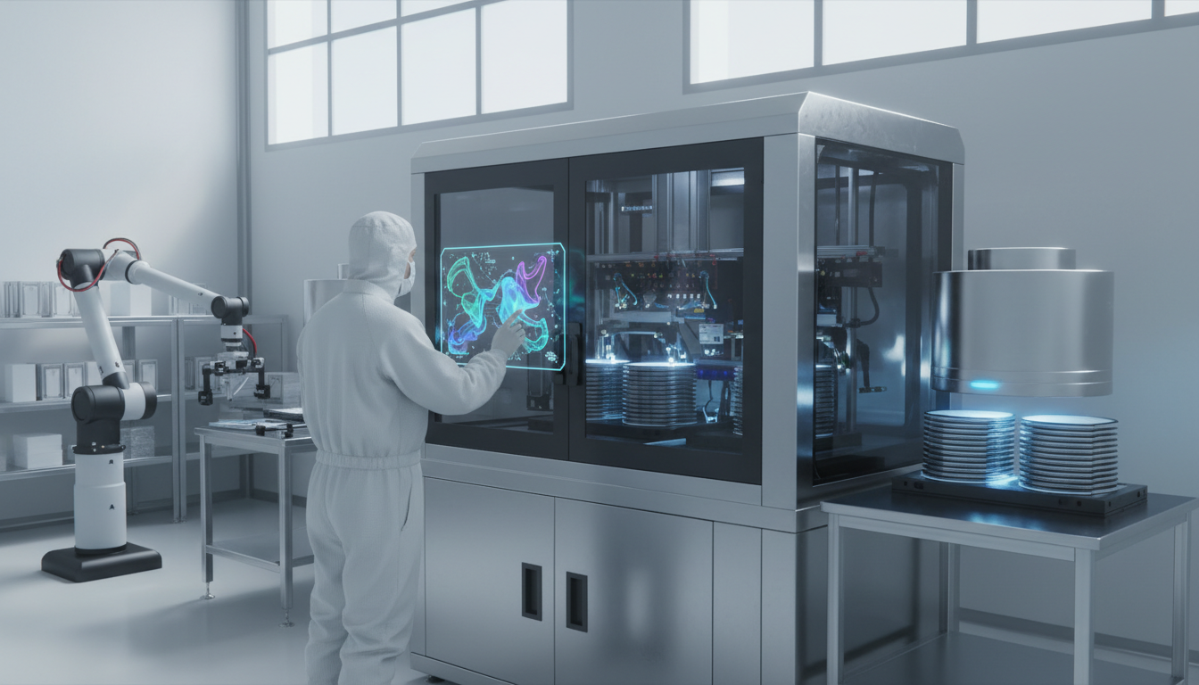
Scalable AI Wafer Inspection
Scalable AI Wafer Inspection represents a pivotal advancement within the Silicon Wafer Engineering sector, integrating artificial intelligence to enhance the precision and efficiency of wafer inspection processes. This innovative approach leverages sophisticated algorithms to analyze wafer quality at unprecedented scales, enabling stakeholders to meet the increasing demands for higher performance and reliability in semiconductor manufacturing. As the sector evolves, the relevance of this concept grows, aligning with broader trends toward automation and AI-led transformations that redefine operational and strategic priorities.
The Silicon Wafer Engineering ecosystem is greatly influenced by Scalable AI Wafer Inspection , as AI-driven practices are fundamentally reshaping competitive dynamics and innovation cycles. By harnessing these technologies, companies can significantly enhance operational efficiency, improve decision-making capabilities, and adapt more swiftly to market changes. However, while the potential for growth is substantial, challenges such as adoption barriers , integration complexities, and evolving stakeholder expectations must be addressed to fully realize the benefits of AI in this context.
Accelerate AI Adoption for Precision Wafer Inspection
Companies in the Silicon Wafer Engineering sector should strategically invest in partnerships focused on Scalable AI Wafer Inspection to enhance operational accuracy and reduce defects. By leveraging AI technologies, businesses can achieve significant cost savings, improve yield rates, and gain a competitive edge in the market.
Transforming Silicon Wafer Engineering: The Role of Scalable AI Wafer Inspection
Implementation Framework
Evaluate current capabilities for AI integration
Establish robust data handling frameworks
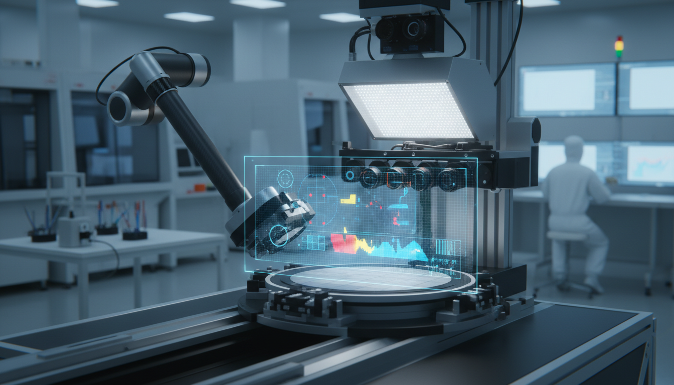
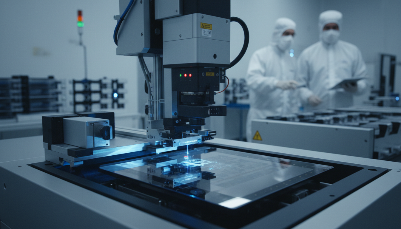
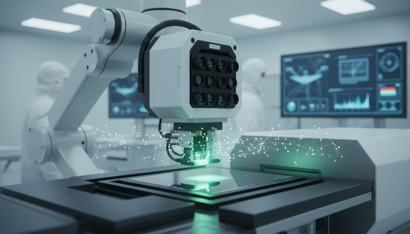
Utilize AI algorithms for inspection
Test AI systems in controlled environments
Expand AI solutions across operations
Conduct a comprehensive evaluation of existing systems' data quality, processing speed, and AI readiness , identifying gaps and areas for enhancement to support scalable AI wafer inspection processes effectively and efficiently.
Internal R&D
Develop and implement a structured data management system that ensures high-quality, accessible data for AI algorithms, enabling accurate inspections and informed decision-making in the silicon wafer engineering domain.
Technology Partners
Select and integrate advanced machine learning algorithms tailored for wafer inspection tasks, enabling real-time defect detection and analysis, which enhances throughput and minimizes waste in silicon wafer production .
Industry Standards
Conduct pilot projects to validate AI solutions in controlled settings, assessing their effectiveness in identifying defects and improving inspection speed, thereby minimizing risks before full-scale implementation in production lines.
Cloud Platform
Gradually scale successful AI solutions across all inspection processes, ensuring that teams are trained and systems are optimized, which enhances overall efficiency and quality assurance in wafer production .
Internal R&D
Best Practices for Automotive Manufacturers
Implement Predictive Maintenance Strategies
- Impact : Reduces unexpected equipment failures
Example : Example: A semiconductor fabrication plant uses AI to predict equipment failures based on historical data, reducing unexpected downtimes by 30% and saving thousands in emergency repairs. - Impact : Lowers maintenance costs significantly
Example : Example: By implementing AI-driven predictive maintenance, a wafer manufacturing facility cut its maintenance budget by 25%, allowing funds to be diverted to R&D initiatives. - Impact : Improves production line uptime
Example : Example: An electronics manufacturer enhanced production line uptime by 40% after deploying AI tools that forecast maintenance needs, allowing preemptive actions to be taken. - Impact : Enhances equipment lifespan and reliability
Example : Example: An AI system analyzes wear patterns on machines, leading to a 20% increase in the average lifespan of critical equipment within the wafer fabrication process.
- Impact : High initial investment for technology
Example : Example: An AI initiative at a wafer production facility stalls due to an unexpected $500,000 integration cost with existing legacy systems, prompting a reevaluation of the project timeline. - Impact : Potential integration with legacy systems
Example : Example: A company faces delays in AI implementation because their outdated equipment cannot effectively interface with new AI technologies, leading to project setbacks and increased costs. - Impact : Need for skilled personnel
Example : Example: Several skilled workers in a semiconductor factory resist AI technologies, fearing job displacement, which creates tension and slows down the adoption process. - Impact : Ongoing data management requirements
Example : Example: A wafer manufacturer struggles with inconsistent data quality, which hinders the performance of its AI systems, ultimately leading to inaccurate defect detection and increased waste.
Enhance Data Collection Techniques
- Impact : Enables real-time monitoring of processes
Example : Example: A silicon wafer manufacturer enhances its data collection techniques by integrating IoT sensors, allowing real-time monitoring of production parameters, which reduces defects by 15%. - Impact : Improves data accuracy and reliability
Example : Example: By upgrading data collection methods, a fab facility increased the accuracy of defect reports from 70% to 95%, directly impacting quality control decisions and reducing waste. - Impact : Facilitates better decision-making
Example : Example: A wafer production line uses enhanced data collection techniques to feed real-time information into AI systems, resulting in a 20% improvement in decision-making speed. - Impact : Supports advanced predictive analytics
Example : Example: By improving data collection, a semiconductor company successfully implemented predictive analytics, leading to a 25% reduction in scrap rates during production.
- Impact : Risk of data overload
Example : Example: An AI-driven wafer inspection system generates vast amounts of data, overwhelming analysts and causing critical insights to be overlooked amid the noise. - Impact : Challenges in data integration
Example : Example: A semiconductor company faces challenges integrating data from multiple sources, leading to delays in analysis and decision-making that impact production efficiency. - Impact : Potential cybersecurity threats
Example : Example: Cybersecurity incidents expose sensitive data from an AI system, raising significant concerns among stakeholders and prompting a review of data protection measures. - Impact : Dependence on data infrastructure
Example : Example: An outdated data infrastructure leads to inconsistent data feeds into an AI model, causing the model to make inaccurate predictions and increasing defect rates.
Train Workforce on AI Tools
- Impact : Enhances employee adaptability and skills
Example : Example: A silicon wafer company invests in training programs for employees on AI tools, resulting in a 30% boost in productivity as workers become adept at using new technologies. - Impact : Boosts overall productivity and efficiency
Example : Example: After comprehensive AI tool training, a wafer fabrication plant sees a 40% reduction in employees' resistance to technology changes, fostering a more innovative workplace culture. - Impact : Reduces resistance to new technologies
Example : Example: Training sessions on AI enhance the skills of technicians, leading to a 25% improvement in process efficiency as they effectively leverage data insights for decision-making. - Impact : Encourages a culture of continuous improvement
Example : Example: By upskilling their workforce, a semiconductor manufacturer cultivates a culture of continuous improvement, leading to significant enhancements in overall operational performance.
- Impact : Training costs can be substantial
Example : Example: A wafer manufacturing facility faces a budget strain from extensive training programs on AI, leading to delays in other operational improvements due to resource reallocation. - Impact : Varied learning curves among employees
Example : Example: Varied learning curves among employees cause frustration, as some adapt quickly to AI tools while others struggle, creating a divide in team performance and morale. - Impact : Potential for skill obsolescence
Example : Example: A company’s investment in AI training risks obsolescence if new technologies emerge, resulting in potential wasted resources and the need for ongoing training. - Impact : Resistance from long-tenured employees
Example : Example: Long-tenured employees resist new AI technologies despite training, believing their traditional methods are superior, causing friction and slowing down team adoption of innovations.
Optimize Inspection Algorithms
- Impact : Increases defect detection rates significantly
Example : Example: By optimizing its defect detection algorithms, a semiconductor manufacturer achieves a 50% increase in detection rates, leading to fewer defective wafers reaching the market. - Impact : Enhances speed of inspections
Example : Example: An AI-driven inspection system at a wafer fab speeds up inspections by 30%, allowing the facility to meet peak production demands without sacrificing quality. - Impact : Reduces false positives in inspections
Example : Example: After refining their inspection algorithms, a silicon wafer fabrication plant reports a 20% reduction in false positives, which streamlines the inspection process and reduces waste. - Impact : Supports continuous process optimization
Example : Example: Continuous optimization of inspection algorithms allows a wafer manufacturer to adapt to changing production parameters, maintaining consistent quality across varying conditions.
- Impact : Risk of overfitting algorithms
Example : Example: A wafer manufacturing facility experiences product failures due to overfitting of their AI inspection algorithms, which were too finely tuned to historical data, missing new defect types. - Impact : High computational resource requirements
Example : Example: High computational demands for optimizing algorithms lead to increased operational costs, pushing a facility to reconsider its technology investments in AI . - Impact : Dependence on quality training data
Example : Example: A semiconductor company finds its AI algorithms underperforming due to reliance on outdated training data, resulting in quality control issues and increased scrap rates. - Impact : Potential algorithm bias issues
Example : Example: Algorithm bias in inspections leads to inconsistent quality checks, causing a backlash from customers when they receive defective products that were incorrectly classified as acceptable.
Utilize Cloud Computing Solutions
- Impact : Enables scalable data processing capabilities
Example : Example: A silicon wafer company adopts cloud computing, allowing them to process large volumes of inspection data quickly, resulting in faster defect analysis and improved decision-making. - Impact : Facilitates enhanced collaboration across teams
Example : Example: Cloud solutions enable a semiconductor manufacturer to enhance collaboration between remote teams, streamlining communication and accelerating problem-solving during the wafer inspection process. - Impact : Reduces IT infrastructure costs
Example : Example: Transitioning to cloud-based systems reduces a wafer fabrication plant’s IT infrastructure costs by 30%, freeing up resources for critical innovation projects. - Impact : Supports advanced analytics and machine learning
Example : Example: Utilizing cloud computing allows for advanced analytics that predict potential defects in production, enabling proactive measures that save time and money in the manufacturing process.
- Impact : Risk of data loss during migration
Example : Example: A wafer production facility experiences data loss during migration to the cloud, resulting in significant setbacks as they scramble to recover critical inspection data. - Impact : Dependence on internet connectivity
Example : Example: An electronics manufacturer faces downtime and productivity losses due to internet connectivity issues, which disrupt access to essential cloud resources during critical inspection periods. - Impact : Potential vendor lock-in issues
Example : Example: A silicon wafer company grapples with vendor lock-in after committing to a single cloud provider, restricting their flexibility and ability to negotiate better terms in the future. - Impact : Concerns about data security
Example : Example: Security breaches at a cloud service provider expose sensitive wafer inspection data, leading to regulatory scrutiny and damage to the company’s reputation.
Leverage Automated Reporting Systems
- Impact : Streamlines inspection reporting processes
Example : Example: An automated reporting system in a silicon wafer factory accelerates the reporting process, resulting in a 40% reduction in time spent on compiling inspection data for management reviews. - Impact : Enhances accuracy of reports
Example : Example: By implementing automated reporting, a semiconductor manufacturer enhances report accuracy by 25%, which helps in identifying quality trends more effectively. - Impact : Improves responsiveness to quality issues
Example : Example: Automated reporting allows a wafer fabrication plant to respond to quality issues within hours instead of days, significantly decreasing the impact of defects on production. - Impact : Supports data-driven decision making
Example : Example: With real-time data feeds to automated reporting systems, a silicon wafer company can make data-driven decisions swiftly, improving overall operational efficiency.
- Impact : High setup and maintenance costs
Example : Example: A silicon wafer company incurs high setup costs for its automated reporting system, leading to budget reallocations that delay other vital projects in the pipeline. - Impact : Training requirements for effective use
Example : Example: Employees struggle to adapt to the new automated reporting tools, requiring additional training and support that temporarily diverts resources from production. - Impact : Potential for system malfunctions
Example : Example: A system malfunction in the automated reporting tool leads to incorrect data being reported, causing confusion and operational inefficiencies in the wafer inspection process. - Impact : Dependence on accurate data input
Example : Example: Inaccurate data input into an automated reporting system results in misleading insights, which causes misinformed decisions and potentially costly production errors.
The path to a trillion-dollar semiconductor industry requires rethinking how manufacturers collaborate, leverage data, and deploy AI-driven automation to handle unprecedented manufacturing complexity in wafer production and advanced packaging.
– John Kibarian, CEO of PDF SolutionsCompliance Case Studies

Seize the opportunity to enhance your processes with AI-driven solutions. Stay ahead of the competition and transform your silicon wafer engineering outcomes now.
Take Test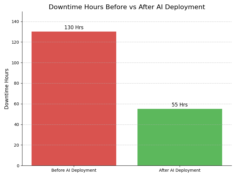
Leadership Challenges & Opportunities
Technical Integration Challenges
Utilize Scalable AI Wafer Inspection technology to create a modular architecture that supports easy integration with legacy systems. Employ standardized APIs and data formats to facilitate seamless data exchange, reducing downtime and operational friction while enhancing overall inspection accuracy.
Cultural Resistance to Change
Foster a culture of innovation by involving teams in the Scalable AI Wafer Inspection implementation process. Conduct workshops and pilot programs that showcase AI capabilities, encouraging buy-in and understanding. This approach cultivates a proactive mindset towards embracing new technologies across the organization.
Resource Allocation Limitations
Implement Scalable AI Wafer Inspection on a phased basis, starting with critical areas that deliver immediate ROI. Leverage cloud solutions to minimize infrastructure costs, allowing for flexible resource management. This strategy ensures optimal use of funds while demonstrating value quickly to secure further investment.
Evolving Regulatory Landscapes
Employ Scalable AI Wafer Inspection's built-in compliance monitoring tools to stay ahead of changing regulations in Silicon Wafer Engineering. Automate documentation and reporting processes, enabling real-time compliance checks and reducing manual errors, thereby ensuring adherence and improving operational efficiency.
Assess how well your AI initiatives align with your business goals
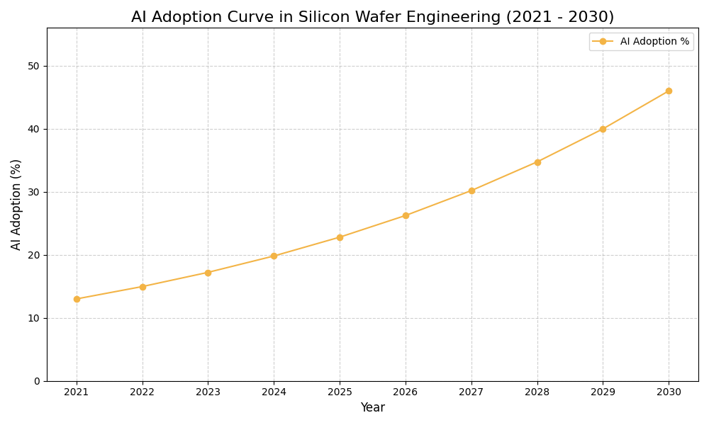
AI Adoption Graph
AI Use Case vs ROI Timeline
| AI Use Case | Description | Typical ROI Timeline | Expected ROI Impact |
|---|---|---|---|
| Automated Defect Detection | Utilizing AI algorithms to identify defects in silicon wafers during production. For example, AI can analyze images from inspection cameras to pinpoint microscopic flaws, significantly reducing manual inspection time and enhancing quality assurance. | 6-12 months | High |
| Predictive Maintenance Scheduling | Implementing AI to predict maintenance needs for wafer fabrication equipment. For example, AI analyzes historical data to anticipate breakdowns, allowing for timely maintenance that minimizes downtime and maximizes production efficiency. | 12-18 months | Medium-High |
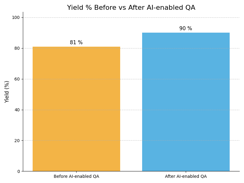
| Yield Optimization Through AI | Leveraging AI to analyze production data and optimize wafer yield. For example, AI can identify patterns that lead to yield losses and suggest adjustments in the manufacturing process, leading to increased output and reduced waste. | 6-12 months | High |
| Real-Time Process Monitoring | Employing AI to monitor wafer processing in real-time. For example, AI systems can analyze sensor data continuously to ensure optimal conditions are maintained, preventing defects and ensuring consistent product quality. | 6-12 months | Medium-High |
Glossary
Work with Atomic Loops to architect your AI implementation roadmap — from PoC to enterprise scale.
Contact NowFrequently Asked Questions
- Scalable AI Wafer Inspection automates quality control processes in wafer production.
- It enhances defect detection accuracy using advanced machine learning algorithms.
- This technology significantly reduces inspection time and operational costs.
- Companies can improve yield rates through real-time data analytics and insights.
- AI-driven solutions provide a competitive edge in the rapidly evolving semiconductor market.
- Start by assessing current inspection processes and technology readiness levels.
- Engage stakeholders to outline specific goals and desired outcomes for implementation.
- Pilot projects can help validate technology performance before wider deployment.
- Training staff on AI tools is crucial for maximizing operational efficiency.
- Partnerships with AI vendors can facilitate smoother integration and support.
- AI improves defect detection speed and accuracy, leading to higher product quality.
- Companies experience reduced operational costs through automation of labor-intensive tasks.
- Enhanced data analytics allows for informed decision-making and process optimization.
- Firms gain a competitive advantage by accelerating time-to-market for new products.
- AI technologies can adapt to changing market demands, ensuring long-term viability.
- Common challenges include data quality issues that can hinder AI performance.
- Resistance to change from staff can slow down the adoption process.
- Integration with legacy systems often requires significant resources and time.
- Ensuring compliance with industry standards can complicate implementation efforts.
- Continuous monitoring and adjustment are necessary to maintain AI effectiveness.
- Firms should consider implementation when existing processes show inefficiencies.
- Market competition can drive the need for faster, more accurate inspection methods.
- Companies planning to scale production benefit from early AI adoption.
- Technological advancements in AI make now an opportune time for investment.
- Assessing internal capabilities can help determine readiness for AI integration.
- AI can identify specific defect types prevalent in silicon wafer production.
- Applications include real-time monitoring of production quality and yield rates.
- Advanced analytics help in predicting equipment failures before they occur.
- AI-driven inspections can streamline compliance with regulatory standards.
- Sector-specific customization ensures that AI tools meet unique industry needs.
- Calculating ROI helps justify investment decisions in new technologies.
- Increased efficiency often translates to significant cost savings over time.
- Measurable outcomes can support continuous improvement initiatives.
- AI can enhance customer satisfaction by reducing time-to-market for products.
- Understanding ROI helps align technology investments with strategic business goals.