
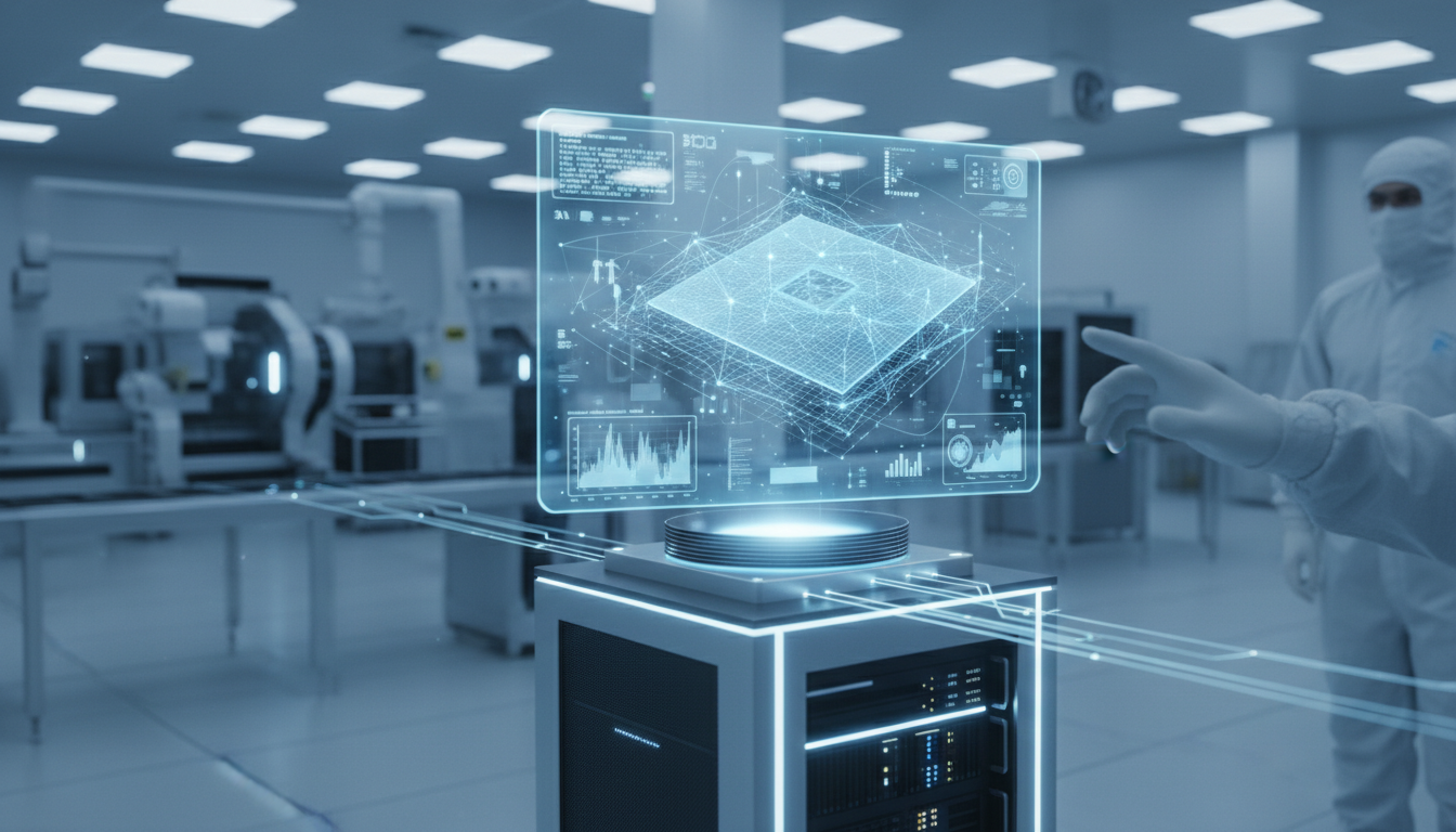
Real Time AI Metrology Wafer
Real Time AI Metrology Wafer represents a pivotal advancement in the Silicon Wafer Engineering arena, where precision measurement and artificial intelligence converge. This innovative concept harnesses AI technologies to enhance metrology processes, ensuring real-time data accuracy and reliability. As industry stakeholders grapple with the complexities of modern semiconductor manufacturing, adopting this approach is vital for maintaining quality and operational excellence. It embodies a broader shift towards AI-led transformations, reshaping strategic priorities and fostering a culture of continuous improvement.
In the evolving ecosystem of Silicon Wafer Engineering , the significance of Real Time AI Metrology Wafer cannot be overstated. AI-driven methodologies are redefining competitive landscapes, pushing the boundaries of innovation and enhancing collaboration among stakeholders. The integration of AI into metrology processes leads to improved efficiency, informed decision-making, and a forward-looking strategic direction. While the prospects of this technology promise substantial growth opportunities, challenges such as adoption barriers , integration complexities, and shifting expectations remain critical considerations for organizations aiming to thrive in this transformative environment.
Leverage Real Time AI Metrology for Competitive Edge
Silicon Wafer Engineering companies should strategically invest in Real Time AI Metrology Wafer technologies and form partnerships with AI specialists to optimize production processes. Implementing AI-driven solutions is expected to enhance precision, reduce costs, and accelerate time-to-market, thereby creating significant competitive advantages.
How Real-Time AI Metrology is Revolutionizing Silicon Wafer Engineering?
Implementation Framework
Identify trends in wafer performance metrics
Deploy machine learning for real-time analysis
Enhance workflows with AI integration
Utilize AI for ongoing monitoring
Conduct thorough data analysis to identify performance trends and anomalies in wafer metrics, leveraging AI algorithms. This enhances predictive maintenance and optimizes production processes, ensuring higher quality outcomes and reduced waste.
Industry Standards
Integrate advanced machine learning algorithms into metrology systems to facilitate real-time data analysis and decision-making. This increases operational efficiency, reduces downtime, and enhances product quality through immediate insights.
Technology Partners
Streamline production workflows by automating routine tasks using AI technologies. This minimizes manual intervention, reduces error rates, and significantly speeds up the production process, thus enhancing overall operational efficiency.
Cloud Platform
Establish continuous monitoring systems powered by AI to track the performance of metrology equipment. This proactive approach allows for immediate adjustments, minimizing disruptions and ensuring sustained production quality over time.
Internal R&D
Best Practices for Automotive Manufacturers
Implement Real-time Data Analytics
- Impact : Improves decision-making speed and accuracy
Example : Example: A semiconductor manufacturer deploys AI analytics on wafer data , enabling engineers to detect anomalies instantly. This leads to faster corrective actions, reducing defects by 20% within the first month. - Impact : Enhances predictive maintenance capabilities
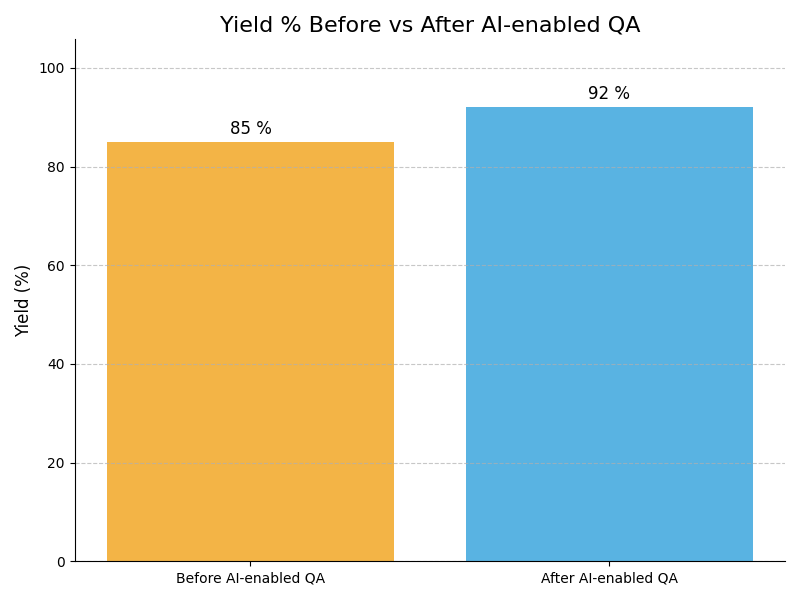
Example : Example: An advanced metrology system predicts equipment failures before they occur, allowing the facility to schedule maintenance proactively, thus avoiding unexpected downtimes and increasing overall productivity. - Impact : Increases yield through real-time adjustments
Example : Example: A solar panel manufacturer uses AI to analyze real-time performance data, making immediate adjustments to processes, which increases yield by 15% during peak production times. - Impact : Boosts data-driven innovation culture
Example : Example: By integrating real-time data visualization, a silicon wafer facility fosters a culture of innovation, encouraging teams to rapidly test and implement new production techniques.
- Impact : High initial investment for technology adoption
Example : Example: A leading chipmaker hesitates to invest in AI systems due to the high costs associated with new hardware and software, ultimately delaying their competitive advantage in the market. - Impact : Potential data integrity issues
Example : Example: Inaccurate sensor data during initial AI implementation led to flawed insights, causing a significant production batch to be scrapped, resulting in financial losses. - Impact : Integration complexities with legacy systems
Example : Example: A silicon wafer factory struggles to integrate new AI systems with outdated machinery, causing delays in achieving promised efficiencies and affecting overall production timelines. - Impact : Dependence on skilled workforce for maintenance
Example : Example: A company finds itself reliant on a small group of data scientists for AI system maintenance, leading to operational risks when the team faces turnover issues.
Enhance Workforce Training Programs
- Impact : Boosts employee confidence in AI systems
Example : Example: A silicon wafer plant implements a comprehensive training program on AI tools, empowering employees to utilize the systems confidently, resulting in a 30% decrease in operational errors within six months. - Impact : Fosters a culture of continuous learning
Example : Example: Regular training sessions on AI methodologies enhance team collaboration and innovation, promoting a learning culture that drives continuous improvement in production processes. - Impact : Improves operational efficiency through skilled labor
Example : Example: By enhancing workforce training, a manufacturer reduces the need for supervision, allowing skilled workers to take initiative, increasing productivity by 25% during peak periods. - Impact : Reduces errors caused by human oversight
Example : Example: Training initiatives focused on AI applications lead to a significant reduction in errors, as workers become adept at identifying issues before they escalate, saving both time and resources.
- Impact : Training costs can escalate quickly
Example : Example: A company underestimates the budget required for comprehensive AI training, leading to insufficient resources and ultimately a less knowledgeable workforce that struggles with new systems. - Impact : Employee resistance to new technologies
Example : Example: Some employees resist adopting AI tools, fearing job displacement, which slows down the overall implementation process and diminishes expected efficiency gains in the factory. - Impact : Knowledge gaps may persist post-training
Example : Example: After training, several employees still lack confidence in using AI systems due to complex interfaces, causing persistent knowledge gaps that hinder productivity. - Impact : Potential for skill obsolescence over time
Example : Example: As AI technology evolves, a company's training program fails to keep pace, leading to skill obsolescence among workers who are not updated on the latest tools and methodologies.
Invest in Robust Data Infrastructure
- Impact : Facilitates seamless data integration
Example : Example: A leading semiconductor firm invests in a cloud-based data platform, allowing real-time access to critical production data, which improves decision-making processes and operational responsiveness significantly. - Impact : Improves data accessibility for analysis
Example : Example: By enhancing their data infrastructure, a silicon wafer manufacturer achieves better data security compliance, reducing the risk of breaches and protecting sensitive intellectual property. - Impact : Enhances data security and compliance
Example : Example: A robust data infrastructure supports seamless integration of various AI systems, allowing for improved analytics and faster adjustments to manufacturing processes, leading to a 15% increase in efficiency. - Impact : Supports scalable AI solutions
Example : Example: As a factory scales production, the upgraded data infrastructure easily accommodates larger datasets, enabling effective AI solutions that drive innovation without compromising performance.
- Impact : High costs associated with infrastructure upgrades
Example : Example: A wafer fabrication facility faces budget overruns due to unanticipated costs related to upgrading their data infrastructure, delaying AI implementation and risking competitive positioning. - Impact : Potential for data silos to develop
Example : Example: Without proper planning, data silos emerge between different departments, limiting the effectiveness of AI analytics and preventing a holistic view of production data. - Impact : Complexity in data migration processes
Example : Example: A company struggles with lengthy data migration processes when upgrading to a new system, which disrupts ongoing operations and leads to temporary inefficiencies. - Impact : Reliance on third-party vendors for support
Example : Example: A silicon wafer manufacturer becomes overly reliant on a third-party vendor for data management, leading to vulnerabilities and delays in updating critical systems and protocols.
Adopt Agile Project Management
- Impact : Enhances responsiveness to market changes
Example : Example: A silicon wafer engineering team adopts agile methodologies, enabling them to quickly pivot their strategies based on market feedback, ultimately launching a new product line three months ahead of schedule. - Impact : Improves collaboration among teams
Example : Example: By fostering collaboration through agile practices, teams in a semiconductor plant communicate more effectively, which leads to faster problem resolution and improved overall production quality. - Impact : Facilitates iterative testing and feedback
Example : Example: An agile approach allows a fabrication facility to conduct iterative testing of new AI systems, refining functionalities in real-time, which significantly enhances product reliability before mass production. - Impact : Accelerates time-to-market for innovations
Example : Example: Implementing agile project management enables a company to reduce time-to-market for innovative silicon wafer products, capturing market share faster than competitors who follow traditional models.
- Impact : Initial adjustment period may hinder productivity
Example : Example: A semiconductor company struggles initially with agile methodologies, as teams find it difficult to adapt, leading to temporary drops in productivity during the transition period. - Impact : Requires cultural shift within the organization
Example : Example: Employees resist the cultural shift towards agile, preferring traditional planning methods, which slows down progress and creates friction among team members. - Impact : Risks of scope creep in projects
Example : Example: A project team experiences scope creep due to insufficiently defined roles in an agile environment, leading to budget overruns and delays in project completion. - Impact : Dependence on effective team communication
Example : Example: Effective communication is essential in agile project management, and when a team fails to maintain this, misalignment occurs, jeopardizing project timelines and objectives.
Utilize Predictive Maintenance Strategies
- Impact : Reduces unexpected equipment failures
Example : Example: A silicon wafer production facility implements predictive maintenance on its etching machines, decreasing unexpected breakdowns by 40%, which leads to a more consistent production schedule. - Impact : Lowers maintenance costs significantly
Example : Example: By predicting equipment failures before they occur, a semiconductor manufacturer saves significantly on emergency repair costs, ultimately leading to a 25% reduction in maintenance expenditures. - Impact : Extends lifespan of critical machinery
Example : Example: Predictive maintenance strategies extend the life of critical machinery, allowing a fabrication plant to avoid costly replacements and maintain continuous operations over longer periods. - Impact : Improves operational efficiency and productivity
Example : Example: Implementing predictive maintenance enhances operational efficiency, as machines run optimally, resulting in a 15% increase in overall productivity on the shop floor.
- Impact : Dependence on accurate data collection
Example : Example: A wafer fabrication plant's predictive maintenance system fails due to inaccurate sensor data, causing unexpected equipment failures and highlighting the importance of quality data collection. - Impact : High upfront costs for advanced tools
Example : Example: The costs associated with implementing advanced predictive maintenance tools exceed initial budget estimates, leading to delays in deployment and affecting overall project timelines. - Impact : Integration challenges with legacy systems
Example : Example: Integration with older systems proves challenging, causing delays in realizing the benefits of predictive maintenance strategies in a semiconductor manufacturing environment. - Impact : Potential for over-reliance on technology
Example : Example: A company becomes overly reliant on predictive maintenance technology, neglecting regular manual inspections, which leads to missed signs of wear and unexpected equipment failures.
Leverage AI for Quality Control
- Impact : Significantly improves defect detection rates
Example : Example: An AI-driven quality control system identifies minute defects in silicon wafers that human inspectors typically overlook, raising defect detection rates by 30% and minimizing waste. - Impact : Reduces manual inspection labor costs
Example : Example: By automating inspections with AI, a semiconductor facility reduces manual labor costs associated with quality checks by 20%, reallocating resources to more strategic tasks. - Impact : Enhances consistency in product quality
Example : Example: AI systems ensure consistent quality across production batches, leading to fewer customer complaints and a stronger brand reputation within the semiconductor industry. - Impact : Accelerates the overall inspection process
Example : Example: The speed of AI in inspecting wafers accelerates the overall process, allowing for higher throughput in production while maintaining stringent quality standards.
- Impact : Reliance on AI can lead to complacency
Example : Example: A semiconductor manufacturer finds that a reliance on AI for quality control leads to complacency, with human inspectors missing defects that the AI does not flag, risking product quality. - Impact : Initial setup may disrupt existing workflows
Example : Example: During initial AI setup, existing workflows are disrupted, causing temporary delays in production and requiring teams to adapt to new processes more slowly than anticipated. - Impact : Potential for algorithm bias affecting quality
Example : Example: An AI quality control system exhibits bias in defect detection due to insufficient training data, resulting in some faults being overlooked and affecting overall product quality. - Impact : Costs associated with ongoing AI maintenance
Example : Example: The ongoing costs of maintaining and updating AI algorithms strain the budget of a wafer fabrication plant, leading to financial scrutiny and reevaluation of priorities.
AI will enable analysts to use all available manufacturing data to make decisions much faster, delivering the operational efficiency needed amid skills shortages and complex wafer production.
– John Kibarian, CEO of PDF SolutionsCompliance Case Studies
_case_study.png)
_case_study.png)

Embrace AI-driven solutions to transform your Silicon Wafer Engineering . Gain a competitive edge and elevate your processes to new heights. Don’t fall behind!
Take Test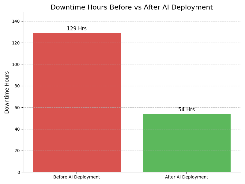
Leadership Challenges & Opportunities
Infrastructure Scalability Issues
Utilize Real Time AI Metrology Wafer to enhance infrastructure scalability by implementing modular architectures. This allows for incremental upgrades and capacity expansion without major disruptions. Real-time data processing ensures timely decision-making, optimizing resource allocation and enhancing overall production efficiency.
Adoption Resistance Culture
Address organizational resistance by demonstrating Real Time AI Metrology Wafer's tangible benefits through pilot projects. Engage employees with hands-on training and transparent communication about the technology's advantages, fostering a culture of innovation and adaptability that embraces data-driven decision making.
High Implementation Costs
Mitigate high initial costs by adopting Real Time AI Metrology Wafer through phased implementations. Start with essential features that deliver immediate ROI, leveraging cloud-based solutions to reduce upfront investments. This strategy allows for gradual scaling while demonstrating financial viability to stakeholders.
Data Security Concerns
Implement Real Time AI Metrology Wafer with robust cybersecurity protocols, including encryption and access controls. Regular audits and compliance checks ensure data integrity and security, fostering trust and reliability in data-driven processes, essential for adhering to industry standards.
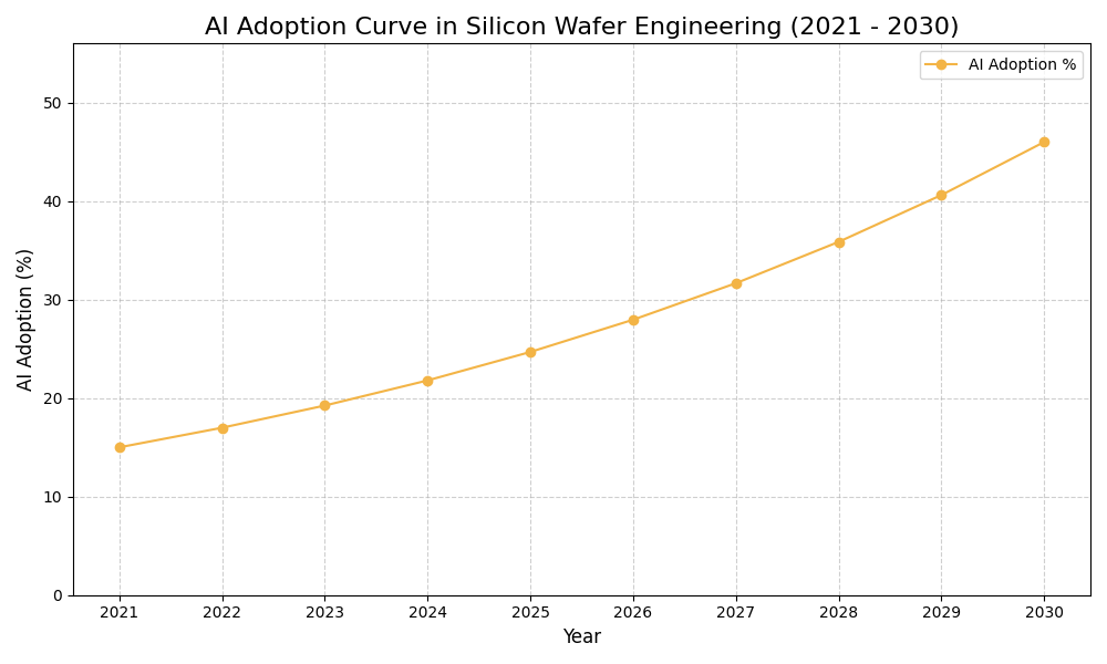
Assess how well your AI initiatives align with your business goals
AI Adoption Graph
AI Use Case vs ROI Timeline
| AI Use Case | Description | Typical ROI Timeline | Expected ROI Impact |
|---|---|---|---|
| Predictive Maintenance for Wafer Equipment | AI algorithms analyze equipment data to predict failures before they occur, minimizing downtime. For example, an AI system can monitor temperature and vibration data from wafer fabrication machines to schedule maintenance proactively, ensuring continuous operation. | 6-12 months | High |
| Yield Optimization in Wafer Production | Utilizing AI to analyze production variables and improve yield rates by identifying patterns and anomalies. For example, AI can assess raw material quality and processing conditions to optimize the fabrication process, increasing overall yield significantly. | 12-18 months | Medium-High |
| Automated Quality Inspection | AI-powered vision systems inspect wafers for defects during production in real-time, reducing manual inspection time. For example, an AI camera can detect microscopic defects on wafers, allowing for immediate corrective actions in the manufacturing process. | 6-9 months | High |
| Process Control with Machine Learning | Implementing AI to dynamically adjust manufacturing processes based on real-time data analysis, enhancing product consistency. For example, machine learning can modify etching times based on current wafer conditions, ensuring uniform quality across batches. | 9-12 months | Medium-High |
Glossary
Work with Atomic Loops to architect your AI implementation roadmap — from PoC to enterprise scale.
Contact NowFrequently Asked Questions
- Real Time AI Metrology Wafer utilizes AI to enhance measurement precision and efficiency.
- It significantly reduces human error through automated data collection and analysis.
- Companies can achieve faster production cycles and improved product quality.
- The technology enables real-time monitoring of wafer characteristics and defects.
- This leads to better decision-making and optimized manufacturing processes.
- Begin with a comprehensive assessment of your current measurement systems.
- Identify key areas where AI can provide measurable improvements and efficiencies.
- Develop a phased implementation plan with specific milestones and objectives.
- Engage cross-functional teams to ensure smooth integration with existing processes.
- Monitor and adjust strategies based on initial results and feedback for ongoing improvement.
- It delivers significant cost savings by improving resource allocation and reducing waste.
- Organizations can enhance product quality through more accurate measurements and insights.
- AI-driven analytics help in identifying trends and anomalies in production.
- This technology provides a competitive edge by accelerating innovation cycles.
- Businesses gain operational agility by adapting quickly to market changes and demands.
- Common obstacles include data integration issues with legacy systems and processes.
- Resistance to change among staff can hinder successful adoption of new technologies.
- Ensuring data quality is crucial for accurate AI-driven insights and actions.
- Adequate training and support must be provided for effective implementation.
- Addressing compliance and regulatory requirements is essential for smooth operations.
- The right time is when your organization aims to enhance production efficiency and quality.
- Consider investment when facing increasing competition and market demand fluctuations.
- Evaluate readiness based on current technological capabilities and workforce skills.
- Timing is ideal during strategic planning cycles to align with long-term goals.
- Investing early can provide a significant advantage as the industry evolves rapidly.
- Organizations must ensure compliance with industry standards and regulations like ISO and SEMI.
- Data privacy and security protocols must be established to protect sensitive information.
- Regular audits and assessments are necessary to maintain compliance and quality standards.
- Documentation of processes and outcomes supports regulatory adherence and transparency.
- Engaging with regulatory bodies can provide guidance on best practices and requirements.