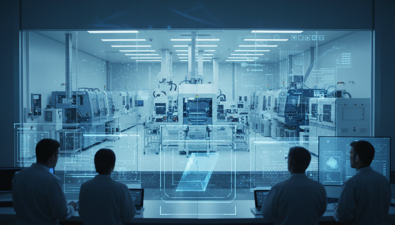
Digital Twin Silicon Wafer Fab
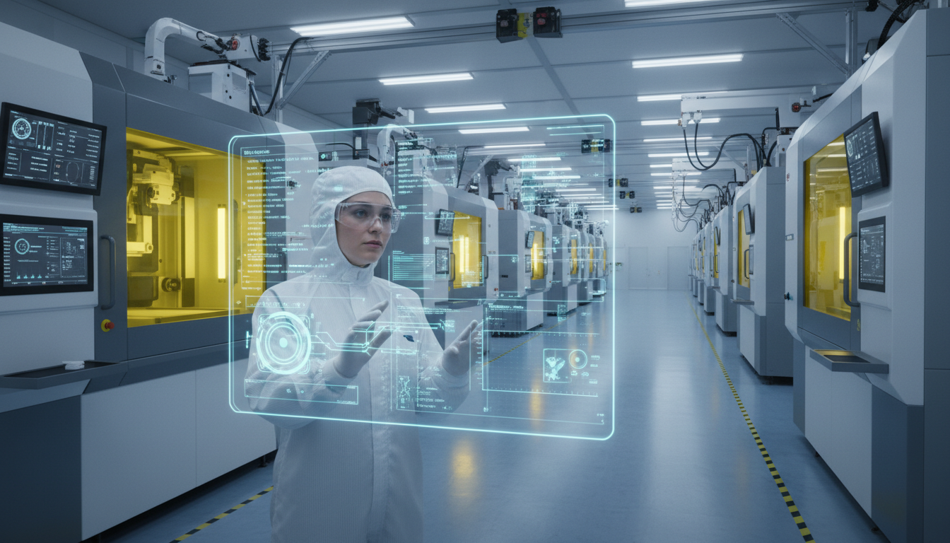
Digital Twin Silicon Wafer Fab refers to the innovative integration of digital twin technology within the Silicon Wafer Engineering sector, enabling a virtual representation of semiconductor manufacturing processes. This concept encompasses the simulation and analysis of wafer fabrication , allowing stakeholders to optimize operations, enhance productivity, and reduce time-to-market. As industries increasingly prioritize digital transformation, the adoption of digital twins aligns seamlessly with AI-led advancements, reflecting a shift towards more data-driven decision-making frameworks and operational strategies.
The ecosystem surrounding Silicon Wafer Engineering is witnessing profound changes due to the implementation of AI-driven practices within Digital Twin Silicon Wafer Fab . These technologies are redefining competitive landscapes, accelerating innovation cycles, and transforming how stakeholders interact. The infusion of AI enhances operational efficiency and supports informed decision-making, ultimately shaping long-term strategic trajectories. While the growth opportunities are abundant, challenges remain, including the complexities of integration and evolving expectations that necessitate careful navigation for successful implementation.
Leverage AI for Competitive Edge in Digital Twin Silicon Wafer Fab
Companies in the Silicon Wafer Engineering industry should strategically invest in partnerships that focus on AI-driven Digital Twin technologies to enhance operational efficiencies and predictive maintenance. Implementing these AI strategies will yield significant ROI through reduced downtime, improved yield rates, and a stronger competitive position in the market.
How AI is Transforming Digital Twin Technologies in Silicon Wafer Fabs?
Implementation Framework
Implement AI technologies for data analysis
Create digital twins of fabrication processes
Set up real-time data monitoring systems
Enhance supply chain resilience with AI
Educate staff on AI tools and methodologies
Integrate advanced AI systems to analyze wafer fabrication data, enabling predictive maintenance and optimizing production processes. This supports operational efficiency and enhances decision-making through actionable insights, driving competitiveness.
Technology Partners
Develop digital twin models for wafer fabrication processes to simulate real-time scenarios, aiding in process optimization and predictive analytics. This enhances agility and responsiveness to operational challenges in silicon wafer engineering .
Internal R&D
Implement real-time monitoring systems to track performance metrics and production outputs. This enables proactive adjustments and improves quality control, ensuring processes align with the digital twin models for optimal results.
Industry Standards
Utilize AI algorithms to analyze supply chain data, enabling predictive insights for inventory management and procurement. This ensures timely availability of materials, reducing delays and improving overall production efficiency.
Cloud Platform
Conduct training programs for staff on AI tools and methodologies relevant to wafer fabrication. This builds a skilled workforce capable of leveraging AI insights, fostering innovation and operational excellence within the organization.
Technology Partners
Best Practices for Automotive Manufacturers
Optimize Data Collection Processes
- Impact : Enhances real-time decision-making capabilities
Example : Example: A silicon wafer fab utilizes IoT sensors to gather real-time data on equipment performance, allowing operators to make informed decisions that cut production delays and boost output by 15%. - Impact : Improves overall production efficiency
Example : Example: By implementing advanced data collection techniques, a factory reduces scrap rates by 20%, resulting in significant cost savings and improved resource utilization across operations. - Impact : Reduces material waste significantly
Example : Example: AI analyzes collected data to predict when maintenance is required, reducing unplanned downtime by 30% and allowing for smoother production schedules. - Impact : Facilitates predictive maintenance scheduling
Example : Example: Real-time analytics enable engineers to adjust processes dynamically, enhancing overall production efficiency by streamlining workflows and minimizing bottlenecks.
- Impact : Data overload can complicate analysis
Example : Example: A wafers manufacturing plant experiences difficulties analyzing huge data volumes, leading to decision-making delays and missed production targets as valuable insights get lost in the noise. - Impact : High costs for advanced data systems
Example : Example: A company invests heavily in advanced data systems only to realize ongoing operational costs exceed budget projections, forcing a reevaluation of financial strategies. - Impact : Inaccurate data collection may mislead
Example : Example: Faulty data collection sensors lead to incorrect process adjustments, causing production disruptions and delays due to misinformed operational changes. - Impact : Integration with legacy systems is challenging
Example : Example: Legacy systems fail to integrate with new AI solutions, resulting in data silos that prevent a holistic view of production processes and hinder efficiency improvements.
Implement Advanced AI Analytics
- Impact : Boosts yield rates significantly
Example : Example: An AI system in a silicon fab analyzes historical data and predicts yield rates, increasing overall output by 25% through optimized process adjustments and effective resource allocation. - Impact : Enhances predictive maintenance accuracy
Example : Example: Predictive maintenance models accurately forecast equipment failures, reducing unplanned downtime by 40% and allowing for proactive scheduling of repairs in a high-tech manufacturing environment. - Impact : Improves defect detection speed
Example : Example: AI algorithms detect defects in real-time, allowing for immediate corrective actions that reduce scrap rates by 15%, ensuring higher quality standards are met consistently. - Impact : Facilitates data-driven decision-making
Example : Example: Data-driven insights enable managers to make informed decisions on resource allocation, increasing production line efficiency by 20% through targeted improvements.
- Impact : Dependence on AI for critical decisions
Example : Example: A semiconductor manufacturer relies heavily on AI outputs for decision-making, leading to operational risks when algorithmic errors occur, resulting in significant production issues. - Impact : Training staff on new technologies
Example : Example: As new AI systems are implemented, employees struggle to adapt, causing lower productivity and operational hiccups that slow down the transition period. - Impact : Data biases may skew results
Example : Example: AI systems trained on biased data lead to skewed defect detection results, compromising quality assurance and requiring additional human oversight to mitigate issues. - Impact : High complexity of AI integration
Example : Example: Complex AI integrations with existing equipment create unforeseen technical challenges that slow down production processes and increase costs during the transition.
Enhance Workforce Training Programs
- Impact : Increases employee competency and confidence
Example : Example: A silicon wafer fab invests in AI-related training for staff, resulting in a 30% increase in employee confidence, leading to faster problem resolution and improved production outcomes. - Impact : Improves collaboration among teams
Example : Example: Cross-training programs foster collaboration between engineers and operators, enhancing workflow efficiency and reducing miscommunication errors that often lead to production delays. - Impact : Boosts innovation through skill enhancement
Example : Example: By enhancing employee skills through targeted training, a company sees a 25% reduction in operational errors, ensuring higher quality standards and reducing rework costs. - Impact : Reduces operational errors significantly
Example : Example: Engaging employees in innovation-focused workshops stimulates creative solutions to existing production challenges, resulting in significant process improvements and competitive advantages.
- Impact : Training programs may be costly
Example : Example: A silicon wafer manufacturer finds that extensive training programs strain budgets, leading to discussions on scaling back, which limits employee development opportunities. - Impact : Resistance to change among employees
Example : Example: Employees resist adopting new AI technologies despite training efforts, causing delays in implementation and lowering morale as staff feel overwhelmed by changes. - Impact : Time-intensive training processes
Example : Example: Training sessions take considerable time away from production, leading to temporary slowdowns that impact output and financial performance during the transition period. - Impact : Skill gaps can still remain
Example : Example: Even after training, some employees struggle to adapt to new AI systems, creating skill gaps that hinder operational efficiency and require additional support.
Leverage Real-time Monitoring
- Impact : Enhances operational visibility across processes
Example : Example: Real-time monitoring systems in a silicon wafer fab increase visibility across production lines, allowing quick adjustments that enhance efficiency and reduce bottlenecks by 20%. - Impact : Improves response times to anomalies
Example : Example: By implementing real-time anomaly detection, a plant can respond to equipment issues within minutes, preventing potential downtime and maintaining smooth operations throughout the day. - Impact : Boosts overall production agility
Example : Example: Continuous monitoring allows production managers to swiftly reallocate resources, boosting overall production agility and improving the response to market demand fluctuations by 15%. - Impact : Facilitates better resource management
Example : Example: Enhanced visibility into resource usage helps managers optimize material allocation, reducing waste and cutting operational costs significantly, leading to increased profitability.
- Impact : High costs for real-time systems
Example : Example: A silicon wafer fab incurs substantial costs when installing real-time monitoring systems, leading to budget constraints that limit other critical investments in technology. - Impact : Potential for system failures
Example : Example: During a system upgrade, unexpected failures in monitoring hardware cause temporary production halts, highlighting vulnerabilities in the infrastructure that need addressing. - Impact : Dependence on accurate sensor data
Example : Example: If sensor data is inaccurate, real-time monitoring can lead to misguided decisions, causing production issues that require time-consuming corrections and potential financial losses. - Impact : Overwhelming data can hinder decisions
Example : Example: An overwhelming amount of real-time data confuses operators, causing decision paralysis and leading to delays in addressing critical operational issues during high-pressure situations.
Utilize Predictive Modeling Techniques
- Impact : Reduces unexpected equipment failures
Example : Example: A silicon wafer facility uses predictive modeling to forecast equipment maintenance needs, reducing unexpected failures by 35% and extending machine lifespans significantly. - Impact : Optimizes production scheduling efficiency
Example : Example: By applying predictive analytics, a fab optimizes its production schedules, leading to a 20% increase in throughput and ensuring timely delivery of products to customers. - Impact : Increases product quality through forecasting
Example : Example: Forecasting models help identify quality issues before they escalate, leading to improved product quality and a 15% reduction in customer complaints over a quarter. - Impact : Facilitates proactive issue resolution
Example : Example: Predictive analytics enables engineers to address potential issues proactively, minimizing production disruptions and ensuring smoother operations across manufacturing lines.
- Impact : Complexity in model development
Example : Example: A silicon wafer manufacturer struggles with developing accurate predictive models, leading to misguided resource allocation and production inefficiencies that affect overall output. - Impact : Over-reliance on predictions
Example : Example: Over-reliance on predictive models results in a lack of human oversight, causing unforeseen production issues when the model fails to account for unique variables. - Impact : Need for continuous data input
Example : Example: Predictive models require continuous data input, and any disruption in data flow can lead to inaccurate forecasts, jeopardizing production schedules and quality assurance. - Impact : Risk of model obsolescence
Example : Example: As technologies evolve, predictive models can become obsolete quickly, requiring constant updates and adjustments that strain operational resources and budgets.
Traditional test wafer approaches are no longer scalable for new process nodes, as they take months or years and cost significant materials and equipment depreciation; comprehensive digital twins enable virtual ramping of processes and designs, providing a better starting point with AI-powered predictive maintenance validated on synthetic data.
– Siemens Semiconductor Executive (speaker in webinar)Compliance Case Studies
_case_study.png)

Unlock unparalleled efficiency and competitive edge with AI-driven Digital Twin solutions. Transform your processes now to stay ahead in Silicon Wafer Engineering .
Take Test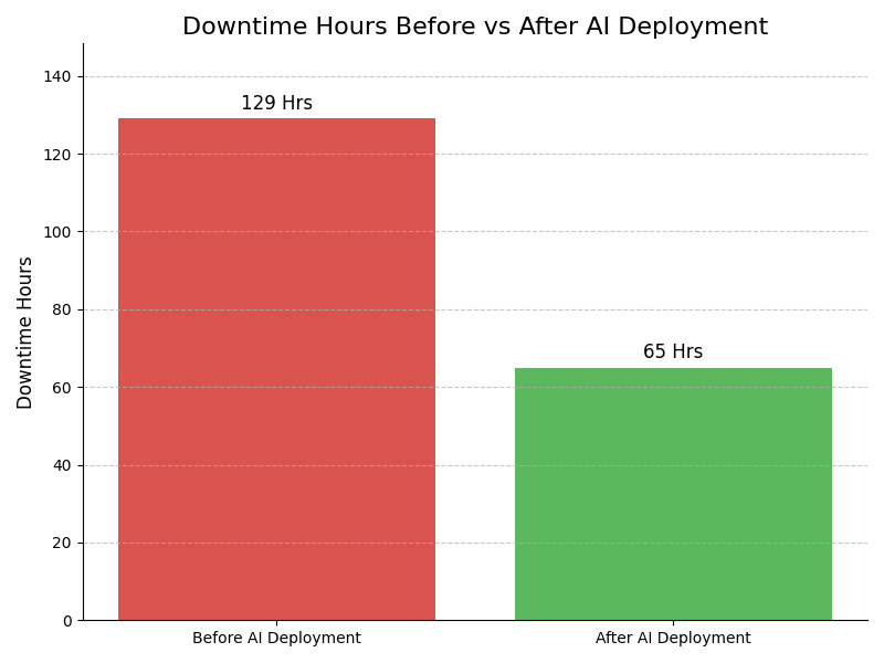
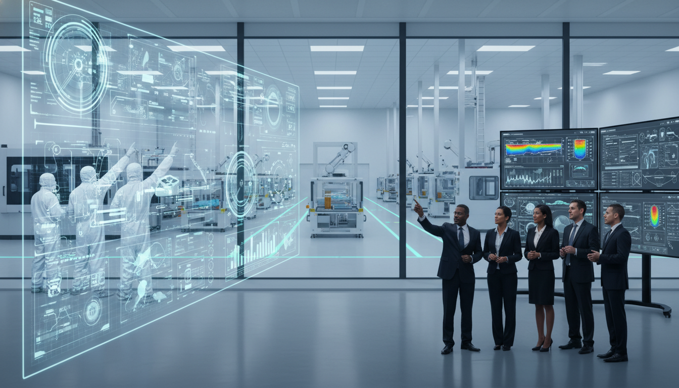
Leadership Challenges & Opportunities
Data Integration Challenges
Utilize Digital Twin Silicon Wafer Fab's robust API capabilities to facilitate seamless data integration across disparate systems. This approach ensures real-time data flow and improves operational visibility, enabling informed decision-making and enhancing overall production efficiency in the Silicon Wafer Engineering process.
Cultural Resistance to Change
Foster a culture of innovation by involving stakeholders in the Digital Twin Silicon Wafer Fab adoption process. Implement collaborative workshops and pilot projects to showcase potential benefits, gradually building buy-in. This inclusive strategy aids in overcoming resistance and encourages a proactive approach to digital transformation.
High Implementation Costs
Minimize initial costs by adopting a phased approach to Digital Twin Silicon Wafer Fab deployment. Start with critical areas that yield quick ROI, utilizing cloud-based models to spread expenses over time. This strategy allows for budget flexibility while demonstrating tangible benefits early in the implementation.
Talent Acquisition Difficulties
Address talent shortages by integrating Digital Twin Silicon Wafer Fab with training platforms that simulate real-world scenarios. Collaborate with educational institutions to create specialized programs, ensuring a steady pipeline of skilled professionals. This proactive approach builds a competent workforce aligned with future industry demands.
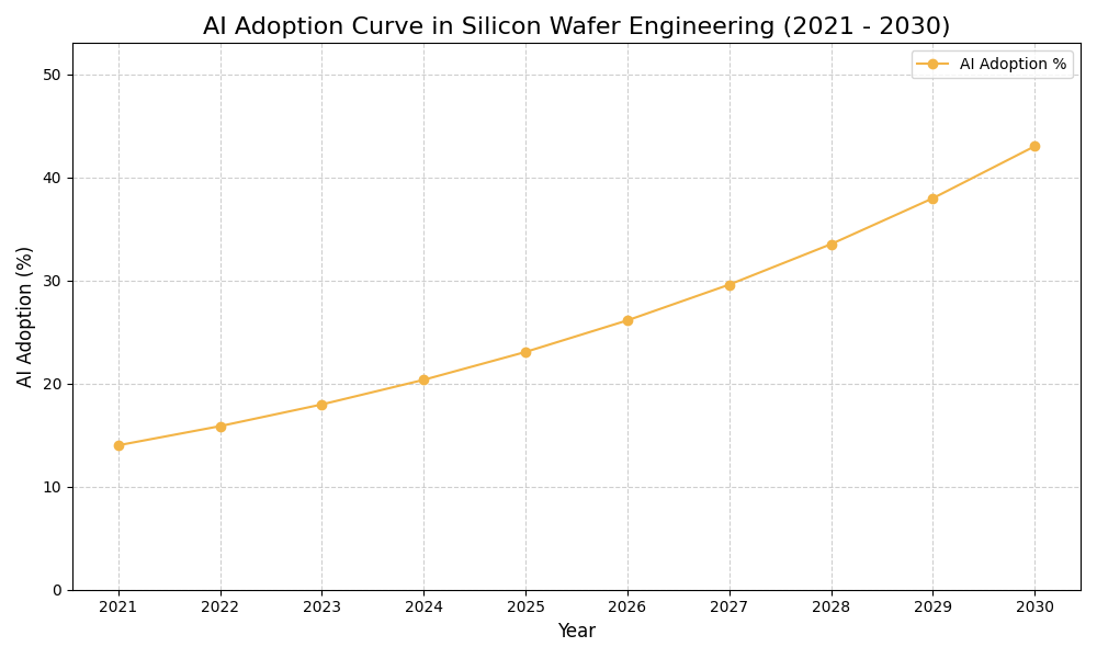
Assess how well your AI initiatives align with your business goals
AI Adoption Graph
AI Use Case vs ROI Timeline
| AI Use Case | Description | Typical ROI Timeline | Expected ROI Impact |
|---|---|---|---|
| Predictive Maintenance for Equipment | AI algorithms analyze sensor data from fabrication equipment to predict failures before they occur. For example, monitoring temperature and vibration data can indicate when a tool needs servicing, reducing downtime and maintenance costs. | 6-12 months | High |
| Yield Optimization through Simulation | Digital twins simulate various fabrication processes to identify optimal settings for maximum yield. For example, adjusting chemical concentrations during etching processes can lead to a significant increase in wafer yield. | 12-18 months | Medium-High |
| Supply Chain Demand Forecasting | AI analyzes market trends and historical data to predict component demand accurately. For example, integrating AI with supply chain management can ensure timely procurement of materials, reducing excess inventory and shortages. | 6-9 months | Medium |
| Process Control Automation | AI tools automate process adjustments in real-time based on live data. For example, adjusting plasma etching parameters based on feedback can maintain quality while improving throughput in fabrication. | 6-12 months | High |
Glossary
Work with Atomic Loops to architect your AI implementation roadmap — from PoC to enterprise scale.
Contact NowFrequently Asked Questions
- Digital Twin Silicon Wafer Fab creates virtual replicas of manufacturing processes.
- It enhances operational efficiency through real-time monitoring and predictive analytics.
- Companies can simulate scenarios to optimize production before implementation.
- This technology reduces downtime by identifying potential issues proactively.
- Ultimately, it leads to improved yield rates and cost savings.
- Begin by assessing current systems and identifying integration points for digital twins.
- Develop a clear roadmap outlining objectives, resources, and timelines for implementation.
- Engage stakeholders to ensure alignment and gather essential input on requirements.
- Pilot projects can help validate the approach before scaling up to full implementation.
- Continuous training and support for teams is crucial for successful adaptation.
- AI optimizes processes by analyzing large datasets for actionable insights.
- Companies can expect improved yield rates and reduced production costs with AI.
- Enhanced quality control measures lead to fewer defects in the final products.
- Business agility increases, allowing quicker responses to market changes.
- Overall, organizations gain a competitive edge through data-driven innovation.
- Resistance to change from staff can hinder successful adoption of new technologies.
- Data integration issues may arise from legacy systems not supporting modern solutions.
- Ensuring data security and compliance with regulations is critical during deployment.
- A lack of skilled personnel can delay the implementation process significantly.
- Addressing these challenges requires proactive planning and stakeholder engagement.
- Organizations should consider adoption when aiming to enhance operational efficiency.
- Timely implementation aligns with business goals focused on innovation and quality.
- Market conditions that demand agility make adoption particularly advantageous.
- Before major capital investments, establishing digital twins can validate processes.
- Regular assessments of technological readiness will guide optimal timing for adoption.
- Digital twins can optimize the design and manufacturing of silicon wafers effectively.
- They enable predictive maintenance, minimizing unplanned downtimes in production.
- Collaboration across teams is enhanced through shared virtual models and insights.
- Quality assurance processes become more effective with real-time monitoring.
- These applications drive innovation and efficiency across the semiconductor industry.
- AI identifies potential risks through predictive models and historical data analysis.
- Automated alerts can notify teams of deviations before they escalate into issues.
- Simulations allow companies to test various scenarios without real-world consequences.
- Data-driven insights support informed decision-making to minimize operational risks.
- Overall, AI enhances resilience by providing a proactive approach to risk management.