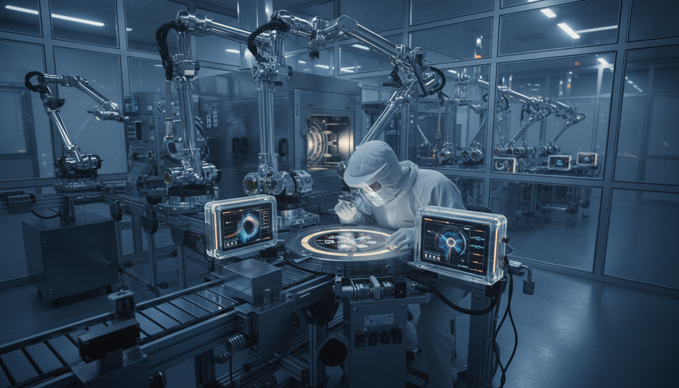
Anomaly Detection Fab Sensors
Anomaly Detection Fab Sensors represent a pivotal innovation in the Silicon Wafer Engineering sector, focusing on identifying irregularities during manufacturing processes. These sensors leverage advanced algorithms to monitor and analyze equipment performance, ensuring the integrity of wafer production . As stakeholders aim for higher yields and reduced downtime, the relevance of these sensors becomes increasingly apparent. This concept aligns with the broader AI-driven transformation within the sector, emphasizing the need for precision and operational efficiency.
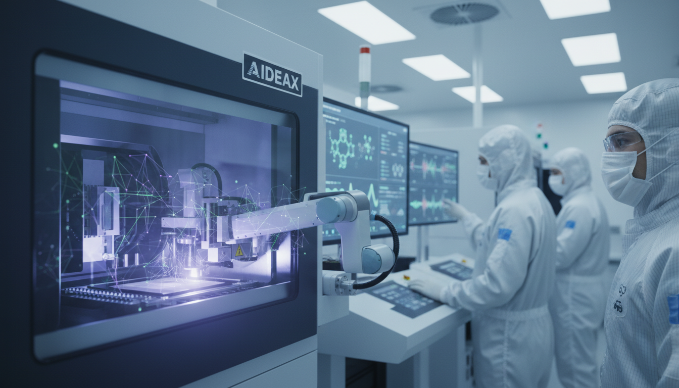
The Silicon Wafer Engineering ecosystem is significantly influenced by AI-driven practices that are reshaping competitive dynamics and innovation cycles. By automating anomaly detection, organizations enhance decision-making processes, driving efficiency and strategic direction. However, the path to successful adoption is not without its challenges, including integration complexities and evolving stakeholder expectations. Nonetheless, the potential for growth remains robust, as businesses navigate these hurdles to leverage technology for greater operational excellence.
Leverage AI for Enhanced Anomaly Detection in Fab Sensors
Silicon Wafer Engineering companies should strategically invest in partnerships focused on AI-driven Anomaly Detection Fab Sensors to optimize their manufacturing processes. Implementing these advanced technologies is expected to yield significant operational efficiencies, reduced downtime, and a stronger competitive edge in the market.
How AI is Revolutionizing Anomaly Detection in Silicon Wafer Engineering
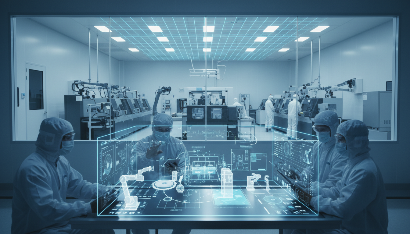
Implementation Framework
Identify relevant data streams for AI
Deploy algorithms for anomaly detection
Enhance model accuracy with data
Track AI effectiveness in real-time
Refine models with continuous input
Conduct a comprehensive assessment of existing data sources, ensuring they align with AI-driven anomaly detection objectives. This enhances predictive accuracy and operational efficiency, ultimately boosting wafer quality and yield rates.
Industry Standards
Integrate machine learning algorithms capable of real-time anomaly detection into existing fab sensor systems. This significantly enhances fault prediction, reducing downtime and improving overall manufacturing efficiency and product reliability.
Technology Partners
Utilize historical data to train AI models, focusing on improving accuracy in anomaly detection. This fosters proactive maintenance strategies, reducing operational costs and increasing the reliability of silicon wafer production .
Internal R&D
Establish a system for real-time monitoring of AI performance metrics to evaluate the effectiveness of anomaly detection. Continuous assessment ensures adaptability and responsiveness, enhancing operational throughput and minimizing defects in production.
Cloud Platform
Create mechanisms for continuous feedback from AI systems to refine anomaly detection models. This iterative process enhances predictive capabilities, resulting in higher yield rates and minimizing operational disruptions in fabrication processes.
Industry Standards
Best Practices for Automotive Manufacturers
Implement AI-Driven Insights
- Impact : Enhances defect detection accuracy significantly
Example : Example: A semiconductor fab implements AI analytics to monitor sensor data, improving defect detection accuracy by 30%, which significantly reduces the number of faulty wafers in production. - Impact : Reduces manual inspection time dramatically
Example : Example: Through AI-driven inspection, a silicon wafer manufacturer cuts manual inspection time by 50%, allowing staff to focus on higher-value tasks and improving overall productivity. - Impact : Increases yield and reduces waste
Example : Example: An AI system identifies patterns in production downtimes, enabling a semiconductor plant to increase yield by 20% while minimizing material waste during processes. - Impact : Facilitates predictive maintenance scheduling
Example : Example: AI algorithms predict equipment failures before they occur, allowing a fab to schedule maintenance proactively, reducing unplanned downtime by 40% and increasing operational efficiency.
- Impact : High initial investment for implementation
Example : Example: A leading wafer fabrication facility delays AI integration due to unexpected costs related to hardware upgrades, significantly affecting their project timeline and budget. - Impact : Data quality issues may arise
Example : Example: A data analysis error in the AI system leads to incorrect defect classifications, resulting in production delays and increased costs due to rework. - Impact : Integration with legacy systems is challenging
Example : Example: During AI system rollout, a silicon wafer manufacturer struggles to integrate new AI tools with outdated machinery, hampering operational efficiency and causing project overruns. - Impact : Dependence on skilled personnel for management
Example : Example: A fab faces operational disruptions because the AI system requires specialized personnel for management, which creates a skills gap and delays response to anomalies.
Optimize Sensor Data Utilization
- Impact : Increases real-time monitoring capabilities
Example : Example: A silicon wafer manufacturing plant installs advanced sensors that feed real-time data into AI systems, allowing engineers to monitor production processes continuously and identify anomalies as they occur. - Impact : Improves data-driven decision-making
Example : Example: A semiconductor company leverages AI to analyze sensor data trends, leading to informed decision-making that reduces production errors by 25% and enhances product quality. - Impact : Enhances predictive maintenance strategies
Example : Example: By using AI to analyze data from various sensors, a fab improves predictive maintenance scheduling, reducing equipment failure rates by 30% and increasing production uptime significantly. - Impact : Boosts overall operational efficiency
Example : Example: Real-time data analytics enhances operational efficiency within a fab, leading to a 15% overall increase in throughput while maintaining quality standards.
- Impact : Inconsistent data from varying sensor types
Example : Example: A silicon wafer manufacturer experiences data inconsistency due to varied sensor types, causing confusion in AI outputs and leading to increased defect rates during production. - Impact : Potential for system overload during peak usage
Example : Example: An AI monitoring system malfunctions when too many sensors send data simultaneously, resulting in system overload and halting production lines during peak manufacturing hours. - Impact : Challenges in data interpretation and analysis
Example : Example: Engineers at a semiconductor fab struggle to interpret complex data generated by AI, leading to incorrect assumptions about defect origins and increased operational costs. - Impact : Risk of sensor malfunctions affecting outputs
Example : Example: A malfunctioning sensor leads to erroneous data being fed into the AI system, resulting in false defect alerts and unnecessary shutdowns of production lines, causing significant delays.
Establish Continuous Learning Framework
- Impact : Enhances AI model accuracy over time
Example : Example: A silicon wafer fabrication facility implements a continuous learning framework for its AI models, increasing defect detection accuracy by 20% over six months as models adapt to new data. - Impact : Adapts to evolving manufacturing environments
Example : Example: An AI system in a semiconductor plant continuously learns from operational data, ensuring it remains effective even as production processes evolve, leading to a 15% reduction in anomaly occurrence. - Impact : Increases resilience against anomalies
Example : Example: By regularly updating their AI algorithms with new data, a fab increases its resilience against anomalies, resulting in a significant decrease in false positives during inspections. - Impact : Fosters innovation through feedback loops
Example : Example: Feedback loops from production teams generate innovative solutions, enhancing the AI system's capabilities and leading to a 10% improvement in overall operational efficiency.
- Impact : Risk of model stagnation without updates
Example : Example: A semiconductor manufacturer faces stagnation in AI performance due to lack of updates, resulting in declining accuracy rates and increased production defects over time. - Impact : Dependence on historical data for learning
Example : Example: An AI model trained on outdated data struggles to adapt to new processes in a fab, leading to poor anomaly detection and unnecessary production halts due to false alarms. - Impact : Increased complexity in system management
Example : Example: The complexity of managing continuously learning AI systems overwhelms existing staff, causing operational disruptions and increasing reliance on external consultants for support. - Impact : Need for ongoing training and resources
Example : Example: Continuous training requirements strain resources at a fab, leading to delays in AI model improvements and impacting overall productivity and efficiency.
Incorporate Multi-Sensor Fusion
- Impact : Enhances detection capabilities across processes
Example : Example: A silicon wafer fab combines data from optical and thermal sensors using AI, enhancing detection capabilities and resulting in a 25% reduction in missed anomalies during inspections. - Impact : Improves anomaly classification accuracy
Example : Example: By implementing multi-sensor fusion, a semiconductor manufacturing facility improves classification accuracy of defects by 30%, leading to more effective quality control measures. - Impact : Reduces false positive rates significantly
Example : Example: AI algorithms processing data from multiple sensors reduce false positive rates by 40%, allowing production teams to focus on genuine issues rather than unnecessary inspections. - Impact : Facilitates comprehensive monitoring solutions
Example : Example: A comprehensive monitoring solution integrating various sensors provides real-time insights, resulting in a 15% increase in overall production efficiency within the fab.
- Impact : Increased complexity in system integration
Example : Example: A silicon wafer manufacturer faces delays in production due to increased complexity in integrating multiple sensor types, impacting overall project timelines and costs. - Impact : Higher costs associated with sensor implementation
Example : Example: The costs associated with implementing multi-sensor systems exceed initial budgets, causing financial strain and delaying AI integration within the fab. - Impact : Potential data overload for analysis
Example : Example: A semiconductor facility experiences data overload from multiple sensors, making it difficult for AI systems to process and analyze information effectively, which slows decision-making. - Impact : Challenges in sensor calibration and alignment
Example : Example: Calibration challenges arise when aligning different sensors, leading to inaccurate data inputs for AI, ultimately causing production disruptions and increased defect rates.
Leverage Cloud-Based AI Solutions
- Impact : Facilitates scalable AI deployment
Example : Example: A silicon wafer fabrication facility leverages cloud-based AI solutions to deploy models quickly, allowing for scalability that meets increasing production demands without delays. - Impact : Enhances collaboration across teams
Example : Example: Cloud-based AI enables collaboration between engineering and production teams, resulting in faster problem-solving and a 20% reduction in time-to-market for new products. - Impact : Improves data accessibility and storage
Example : Example: Data stored in the cloud allows engineers easy access to historical production data, enhancing their ability to analyze trends and improve operational efficiency by 15%. - Impact : Reduces on-premises hardware costs
Example : Example: By utilizing cloud solutions, a fab reduces on-premises hardware costs significantly, freeing up budget for further investments in advanced technology and staff training.
- Impact : Dependence on stable internet connections
Example : Example: A silicon wafer manufacturer experiences production halts due to unstable internet connections, impacting the performance of their cloud-based AI systems and causing delays in defect detection. - Impact : Data security concerns with cloud storage
Example : Example: Security breaches in cloud storage lead to sensitive production data exposure, raising significant concerns about data privacy and compliance within the fab . - Impact : Potential latency in data processing
Example : Example: An increase in latency during peak usage times affects data processing speeds, slowing down decision-making and potentially leading to production errors in the semiconductor facility. - Impact : Vendor lock-in with cloud providers
Example : Example: A fab becomes reliant on a single cloud provider, facing challenges with vendor lock-in when trying to switch to a more cost-effective solution, limiting future flexibility.
AI and ML are being implemented for mask and wafer detection and yield optimization in semiconductor manufacturing, increasing engineer productivity.
– Tim Costa, Vice President of Industrial Engineering and Quantum Verticals, NVIDIACompliance Case Studies


Embrace AI-driven solutions for Fab Sensors to enhance precision and efficiency in Silicon Wafer Engineering . Don't miss the chance to lead the industry transformation.
Take Test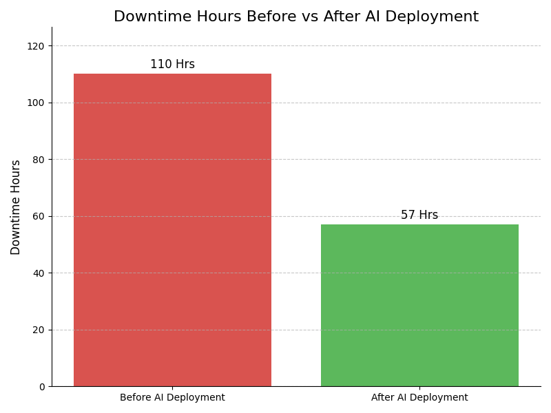
Leadership Challenges & Opportunities
Data Drift Monitoring
Integrate Anomaly Detection Fab Sensors to continuously monitor data drift in real-time during wafer fabrication. This technology enables proactive identification of deviations from established patterns, ensuring consistent quality and performance. By automating alerts, teams can swiftly address issues, minimizing scrap and enhancing yield.
Cultural Resistance to Change
Foster a culture of innovation by demonstrating the value of Anomaly Detection Fab Sensors through pilot projects. Engage teams in the process by showcasing quick wins and involving them in feedback loops. This collaborative approach helps alleviate fears, encouraging acceptance and integration into existing workflows.
High Operational Costs
Implement Anomaly Detection Fab Sensors to optimize resource allocation and reduce operational costs in wafer fabrication. By identifying inefficiencies and predictive maintenance needs, companies can minimize downtime and waste. This leads to significant cost savings while maintaining high production standards and increasing overall efficiency.
Compliance with Industry Standards
Utilize Anomaly Detection Fab Sensors to automate compliance monitoring against industry standards in Silicon Wafer Engineering. This technology provides real-time data analytics and reporting capabilities, ensuring adherence to regulations. By streamlining documentation and improving traceability, organizations can reduce compliance risks and enhance operational transparency.
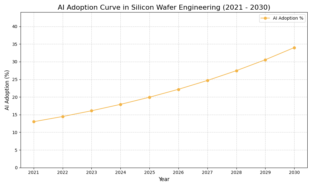
Assess how well your AI initiatives align with your business goals
AI Adoption Graph
AI Use Case vs ROI Timeline
| AI Use Case | Description | Typical ROI Timeline | Expected ROI Impact |
|---|---|---|---|
| Predictive Maintenance for Fab Equipment | AI analyzes sensor data to predict equipment failures, optimizing maintenance schedules. For example, a semiconductor manufacturer uses AI to identify wear patterns in fabrication tools, reducing unplanned downtime by scheduling maintenance before breakdowns occur. | 6-12 months | High |
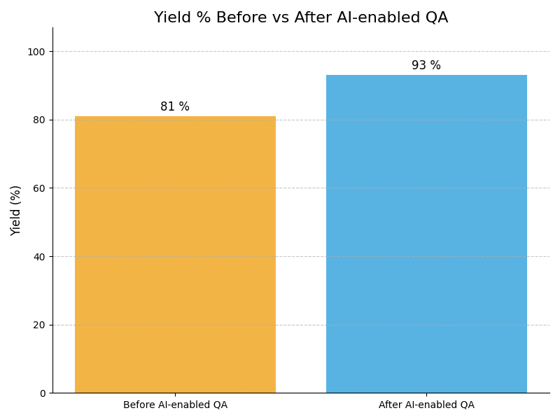
| Quality Assurance through Anomaly Detection | AI identifies deviations in sensor readings, ensuring product quality. For example, a wafer fabrication plant employs machine learning to detect anomalies during etching processes, significantly reducing defects and improving yield rates. | 12-18 months | Medium-High |
| Real-time Process Optimization | AI enables real-time adjustments to fabrication processes based on sensor data, enhancing efficiency. For example, during lithography, AI dynamically adjusts settings to minimize errors, leading to improved throughput and quality. | 6-9 months | Medium |
| Supply Chain Forecasting | AI predicts supply chain disruptions by analyzing sensor trends and external factors. For example, a fab utilizes AI to foresee material shortages by monitoring equipment usage and environmental conditions, allowing proactive procurement strategies. | 12-18 months | Medium-High |
Glossary
Work with Atomic Loops to architect your AI implementation roadmap — from PoC to enterprise scale.
Contact NowFrequently Asked Questions
- Anomaly Detection Fab Sensors utilize AI to identify irregular patterns in data.
- AI enhances detection accuracy by learning from historical data and adapting to changes.
- The technology minimizes false positives, improving overall operational efficiency.
- Effective use leads to quicker resolutions of potential issues, reducing downtime.
- AI-driven sensors provide valuable insights for continuous process improvement.
- Integration requires a thorough assessment of current systems and data flows.
- Collaborating with IT and engineering teams ensures compatibility with existing infrastructure.
- Phased integration helps to mitigate risks and allows for gradual adjustments.
- Training staff on new systems is crucial for seamless adoption and effectiveness.
- Regular evaluations post-integration help identify areas for further optimization.
- Implementing AI enhances efficiency, leading to significant cost savings over time.
- AI-driven insights enable proactive decision-making, improving operational outcomes.
- Companies experience enhanced quality control, resulting in higher customer satisfaction.
- Measurable metrics include reduced downtime and improved throughput rates.
- The competitive advantage gained can lead to increased market share and innovation.
- Common challenges include data quality issues and integration complexities.
- Resistance from staff can hinder adoption, making change management vital.
- Budget constraints may limit the scope of implementation and necessary training.
- Mitigation strategies include pilot testing and phased rollouts to manage risk.
- Maintaining continuous support and updates is essential to address emerging challenges.
- The ideal timing is when existing systems show inefficiencies or increased error rates.
- Consider adoption during a planned technology refresh or digital transformation initiative.
- Assessing market conditions can reveal competitive pressures that necessitate action.
- Seek opportunities for pilot projects when resources allow for experimentation.
- Proactive adoption prepares your organization for future advancements in technology.
- Applications include monitoring wafer fabrication processes for quality assurance.
- AI can detect deviations in production parameters to prevent defects early.
- Predictive maintenance of equipment ensures optimal performance and reduces downtime.
- Regulatory compliance can be enhanced through accurate data tracking and reporting.
- Benchmarking against industry standards ensures competitive positioning and quality.
- Compliance with industry standards is crucial for maintaining product integrity and safety.
- Documentation of AI decision-making processes helps meet regulatory requirements.
- Regular audits of AI systems ensure ongoing compliance with evolving standards.
- Data security measures must comply with regulations to protect sensitive information.
- Collaborating with legal teams can help navigate complex regulatory landscapes.
- Success can be measured through key performance indicators like reduced defects.
- Tracking downtime before and after implementation highlights improvements.
- Employee feedback on usability and efficiency provides qualitative insights.
- Benchmarking against industry standards offers a comparative perspective on performance.
- Regular reviews of operational metrics ensure alignment with strategic goals.