
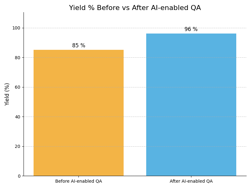
AI Yield Optimization Fab Best
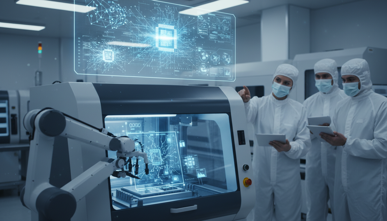
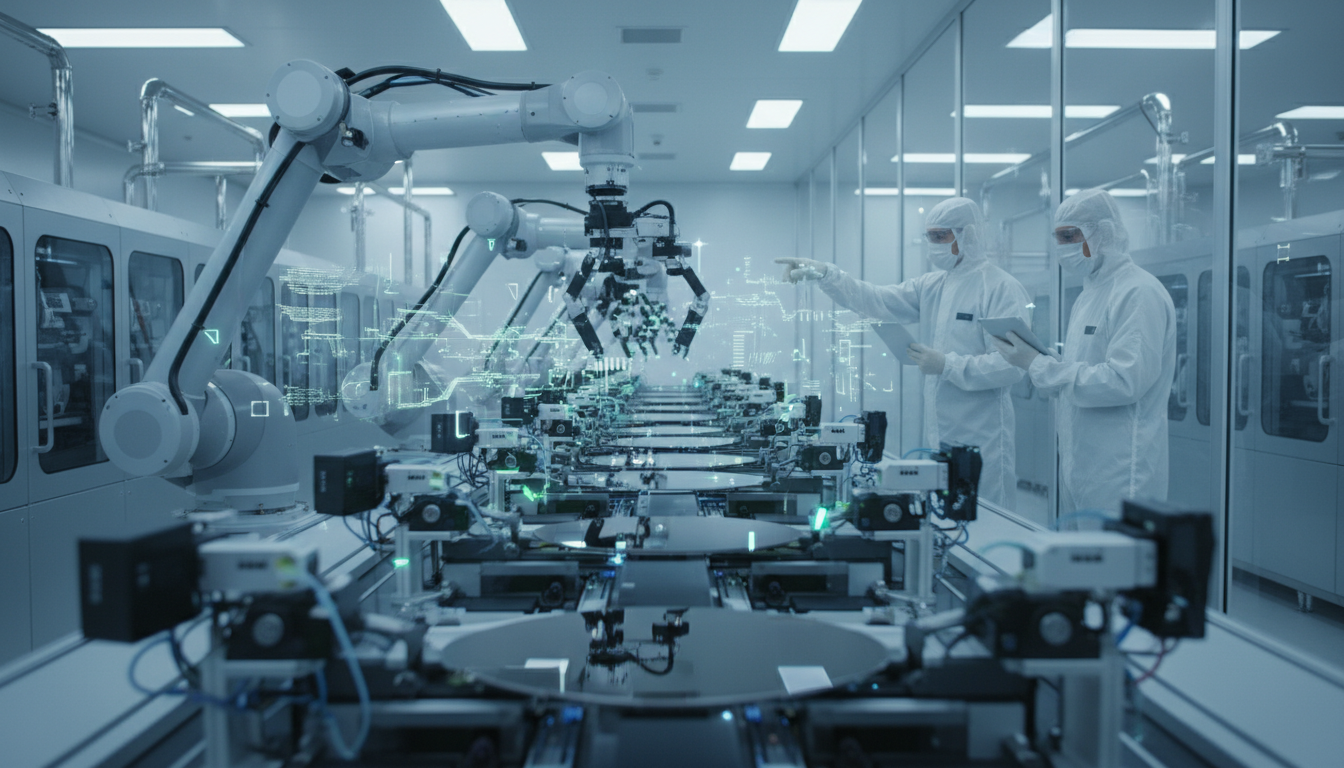
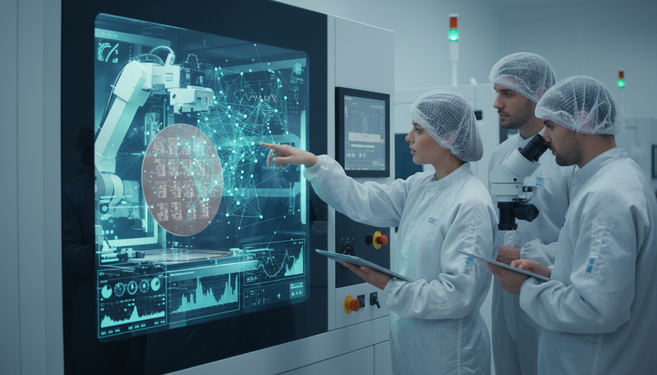
AI Yield Optimization Fab Best refers to the implementation of artificial intelligence techniques in the Silicon Wafer Engineering sector, aimed at enhancing production yields and operational efficiencies. This concept encompasses a range of AI-driven methodologies that optimize processes and decision-making within fabrication facilities. As stakeholders increasingly prioritize automation and data analytics, the integration of AI in yield optimization signifies a crucial shift towards smarter manufacturing practices, aligning with broader trends in digital transformation.
The Silicon Wafer Engineering ecosystem is experiencing a profound transformation due to AI-driven yield optimization practices. These innovations are reshaping competitive dynamics by fostering a culture of continuous improvement and agile decision-making among stakeholders. As companies leverage AI to enhance efficiency and streamline operations, they encounter both significant growth opportunities and challenges. The integration of AI may present barriers such as technological complexity and evolving expectations, necessitating a balanced approach to harness the full potential of these advancements while addressing inherent risks.
Maximize ROI with AI Yield Optimization Strategies
Silicon Wafer Engineering companies should strategically invest in AI-driven yield optimization technologies and form partnerships with leading AI firms to enhance production processes. By implementing these AI strategies, companies can achieve significant operational efficiencies, reduced waste, and a strong competitive edge in the market.
Transforming Silicon Wafer Engineering: The AI Yield Optimization Revolution
Implementation Framework
Evaluate current capabilities for AI integration
Utilize data analytics for informed decisions
Integrate machine learning for predictive insights
Automate processes to increase efficiency
Establish a feedback loop for enhancements
Conduct a thorough assessment of existing technologies and processes to identify gaps in AI readiness , ensuring alignment with strategic goals for yield optimization and identifying potential areas for improvement.
Technology Partners
Integrate advanced data analytics tools to monitor and analyze production processes in real-time, facilitating data-driven decisions that enhance yield optimization and reduce waste in silicon wafer engineering operations.
Industry Standards
Develop and deploy machine learning algorithms to predict equipment failures and optimize production parameters, enhancing yield rates while minimizing downtime and increasing overall productivity in wafer fabrication processes.
Internal R&D
Implement AI-driven automation solutions to streamline workflows in wafer fabrication , reducing manual errors and enhancing process reliability, which contributes to achieving optimal yield performance and operational agility .
Cloud Platform
Create a continuous improvement framework that incorporates AI-driven insights, fostering a culture of innovation and agility within the organization, ensuring sustained yield optimization and adaptability to market changes.
Industry Standards
Best Practices for Automotive Manufacturers
Implement Predictive Maintenance Strategies
- Impact : Minimizes unexpected equipment failures
Example : Example: A silicon wafer fab employs predictive algorithms to analyze machine vibrations, identifying wear patterns that enable timely maintenance, thus preventing unexpected breakdowns and reducing downtime by 30% over six months. - Impact : Extends machinery lifespan significantly
Example : Example: By implementing machine learning models, a wafer manufacturing plant extends the lifespan of critical etching equipment by 25%, ensuring consistent output over longer periods without major upgrades or replacements. - Impact : Reduces maintenance costs over time
Example : Example: A semiconductor facility reduces maintenance costs by 20% through predictive analytics, which allows for scheduled repairs instead of reactive fixes, optimizing resources and labor efficiency significantly. - Impact : Improves overall production reliability
Example : Example: AI-driven predictive maintenance leads to a 40% reduction in unplanned downtime, enhancing production reliability and enabling the company to meet tighter delivery schedules.
- Impact : High initial investment in AI infrastructure
Example : Example: A silicon wafer manufacturer hesitates to invest in AI infrastructure due to the high upfront costs of new sensors and software, impacting their ability to adopt advanced analytics and stay competitive. - Impact : Complexity of data integration processes
Example : Example: Integration issues arise when a new AI system fails to connect with legacy equipment, resulting in production delays and increased operational costs as teams scramble to find workarounds. - Impact : Reliance on accurate historical data
Example : Example: An AI model relies on historical production data that is incomplete, leading to inaccurate predictions and flawed maintenance schedules, which increase operational risks and costs. - Impact : Potential resistance from operational staff
Example : Example: Resistance from staff occurs when operators fear job loss due to AI adoption , causing friction and delays in implementing new systems and processes.
Leverage Real-time Data Analytics
- Impact : Enhances decision-making speed significantly
Example : Example: A silicon wafer production line utilizes real-time analytics to adjust parameters on the fly, decreasing yield loss by 15% as issues are detected and resolved almost instantaneously, enhancing throughput. - Impact : Identifies yield issues quickly and accurately
Example : Example: Real-time data tracking helps a semiconductor company pinpoint yield drop causes within hours, leading to rapid corrective actions that save significant costs and improve production efficiency. - Impact : Optimizes production schedules effectively
Example : Example: By analyzing data in real-time, a fab can adjust its production schedule to accommodate urgent orders, resulting in a 25% increase in customer satisfaction and retention rates. - Impact : Increases responsiveness to market changes
Example : Example: A silicon wafer manufacturer adapts to changing market demands by adjusting production rates in real-time, leading to a 20% reduction in excess inventory and improved cash flow management.
- Impact : Data overload can obscure key insights
Example : Example: A silicon wafer factory experiences data overload, causing critical insights to be buried under irrelevant information, resulting in slower decision-making and potential yield losses as problems go unnoticed. - Impact : Dependence on continuous system uptime
Example : Example: Continuous data analytics systems crash during peak usage, leading to a complete halt in production decisions, which significantly affects output and leads to financial losses. - Impact : Inaccurate data can mislead operations
Example : Example: An AI model misinterprets inaccurate sensor data, leading to errors in operational adjustments that impact production quality, causing costly rework and scrap rates to soar. - Impact : Need for ongoing staff training
Example : Example: Staff struggle to keep up with the rapid pace of new analytics tools, necessitating ongoing training programs that strain budgets and resources, delaying full AI integration.
Utilize Automated Quality Control
- Impact : Reduces human error in inspections
Example : Example: An automated quality control system uses AI to inspect wafers at high speeds, reducing defect rates by 30% compared to manual inspections, ensuring only quality products reach customers. - Impact : Enhances product consistency and quality
Example : Example: A semiconductor manufacturer implements machine vision technology, which enhances inspection accuracy, achieving a 95% consistency rate in quality checks and dramatically improving customer satisfaction. - Impact : Increases inspection speed dramatically
Example : Example: AI-driven inspections in a wafer fab increase inspection speeds by 50%, allowing for faster production cycles while maintaining high quality standards, thus meeting market demands promptly. - Impact : Decreases overall defect rates
Example : Example: Automated quality checks significantly decrease human error, leading to a 40% reduction in defects and enhancing the overall reliability of the production line.
- Impact : Initial setup can disrupt operations
Example : Example: A company faces production delays due to the initial setup of an automated quality control system, disrupting regular workflows and impacting output during implementation. - Impact : Integration with existing processes may fail
Example : Example: Integration challenges arise when automated systems cannot adapt to existing manual inspection processes, causing confusion and inefficiencies that affect production timelines. - Impact : Ongoing maintenance costs can escalate
Example : Example: Following the installation of new automated inspection systems, ongoing maintenance costs exceed initial estimates by 25%, straining the operational budget and requiring reevaluation of financial resources. - Impact : Limited flexibility for unique defects
Example : Example: Automated systems struggle to identify unique defects not accounted for in algorithms, leading to undetected quality issues that negatively impact product reliability and customer trust.
Incorporate AI-driven Process Simulation
- Impact : Enhances design validation processes
Example : Example: A semiconductor fab employs AI-driven process simulations to validate design parameters before production, reducing design errors by 30% and accelerating time-to-market for new products substantially. - Impact : Optimizes resource allocation effectively
Example : Example: By simulating various production scenarios, a wafer manufacturer optimizes resource allocation, achieving a 20% reduction in material waste and improving sustainability metrics without sacrificing quality. - Impact : Reduces development time significantly
Example : Example: AI simulations cut development time in half for new wafer technologies , enabling faster responses to market demands and giving the company a competitive edge in innovation. - Impact : Facilitates better collaboration among teams
Example : Example: Collaborative platforms using AI-driven simulations enhance communication between engineering and production teams, leading to a 25% increase in project completion rates and improved product outcomes.
- Impact : High computational costs for simulations
Example : Example: A silicon wafer engineering firm faces high computational costs when implementing AI simulations, which limits their ability to explore multiple design iterations within budget constraints. - Impact : Complexity may hinder user adoption
Example : Example: Engineers struggle to adopt complex simulation tools, resulting in low utilization rates and missed opportunities for improved design processes and innovation. - Impact : Requires significant historical data
Example : Example: An AI-driven simulation requires extensive historical data to function accurately; when data is incomplete, the simulations yield unreliable results, leading to poor decision-making. - Impact : Potential inaccuracies in simulation models
Example : Example: Inaccuracies in simulation models lead to flawed assumptions about process capabilities, resulting in unexpected production issues that require costly rework and adjustments.
Train Workforce in AI Technologies
- Impact : Boosts employee engagement and morale
Example : Example: A silicon wafer manufacturer trains employees in AI technologies, leading to increased engagement and morale as staff feel empowered to contribute to innovation and improvements in processes. - Impact : Enhances skill sets for future needs
Example : Example: By upskilling the workforce in AI tools, a fab enhances employee skill sets, ensuring they are prepared for future demands and reducing the need for external hiring significantly. - Impact : Reduces resistance to AI adoption
Example : Example: Training programs reduce resistance to AI adoption as employees become familiar with new technologies, resulting in smoother transitions and improved collaboration across teams during implementation. - Impact : Improves overall team productivity
Example : Example: A comprehensive training initiative leads to a 30% boost in overall team productivity, as workers effectively utilize AI tools to enhance workflow efficiency and output quality.
- Impact : Training programs can be costly
Example : Example: A silicon wafer fab incurs significant costs when rolling out extensive training programs for AI technologies, straining the budget and delaying other key initiatives. - Impact : Time-consuming to implement effectively
Example : Example: Implementation of training programs takes longer than anticipated, causing disruptions in daily operations and delaying the adoption of AI tools in production processes. - Impact : Varied employee readiness levels
Example : Example: Employee readiness for AI training varies widely, leading to frustrations among less tech-savvy staff and hindering overall progress and integration efforts. - Impact : Potential knowledge gaps may arise
Example : Example: Knowledge gaps emerge when some employees do not fully grasp new AI tools , resulting in inconsistent usage and underutilization of advanced technologies across the organization.
The 2025–2026 wafer market is shaped by diverging trends across technology nodes. Demand for 300mm wafers remains strong in advanced applications, particularly in AI-driven logic and high-bandwidth memory (HBM), supported by the ongoing adoption of sub-3nm processes, which are driving increased requirements for wafer quality and consistency.
– Ginji Yada, Chairman of SEMI SMG and Executive Office Deputy General Manager, Sales and Marketing Division at SUMCO CorporationCompliance Case Studies

Seize the competitive edge in Silicon Wafer Engineering . Embrace AI-driven yield optimization solutions today and transform your manufacturing outcomes for tomorrow.
Take Test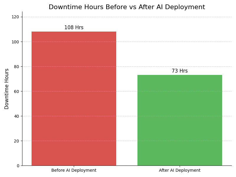
Leadership Challenges & Opportunities
Data Integration Challenges
Utilize AI Yield Optimization Fab Best to create a centralized data hub that integrates disparate sources within Silicon Wafer Engineering. Implement machine learning algorithms to analyze and harmonize data, improving decision-making and process efficiency while ensuring real-time insights across production stages.
Change Management Resistance
Facilitate a cultural shift towards AI Yield Optimization Fab Best through stakeholder engagement and transparent communication. Organize workshops to demonstrate benefits, encouraging adoption. Use change champions within teams to promote success stories, fostering an environment where innovation is embraced and resistance is minimized.
Resource Allocation Issues
Implement AI Yield Optimization Fab Best to optimize resource allocation in Silicon Wafer Engineering. Utilize predictive analytics to forecast demand and adjust resource distribution accordingly, ensuring efficient use of materials and workforce. This approach enhances productivity while minimizing waste, leading to cost savings.
Compliance with Industry Standards
Leverage AI Yield Optimization Fab Best to streamline compliance processes in Silicon Wafer Engineering. Utilize automated reporting and real-time monitoring features to ensure adherence to industry regulations, while machine learning identifies potential compliance risks proactively, simplifying audits and maintaining operational integrity.
Assess how well your AI initiatives align with your business goals
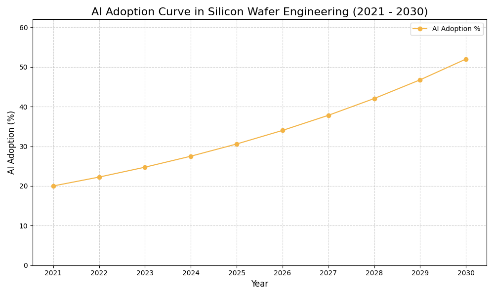
AI Adoption Graph
AI Use Case vs ROI Timeline
| AI Use Case | Description | Typical ROI Timeline | Expected ROI Impact |
|---|---|---|---|
| Predictive Maintenance for Equipment | By utilizing AI algorithms to analyze equipment data, predictive maintenance can forecast potential failures. For example, a semiconductor fab uses machine learning to anticipate when a photolithography tool will need service, minimizing downtime and maintenance costs. | 6-12 months | High |
| Process Parameter Optimization | AI can optimize manufacturing parameters in real-time, improving yield rates. For example, an advanced fab employs AI to adjust etching parameters dynamically, resulting in a 15% increase in wafer yield. | 12-18 months | Medium-High |
| Defect Detection Automation | Leveraging computer vision, AI automates defect detection in wafers, increasing accuracy and speed. For example, a fab uses AI to scan wafers for micro-defects, reducing human error and improving quality control. | 6-12 months | High |
| Supply Chain Optimization | AI enhances supply chain efficiency by predicting material requirements. For example, a semiconductor manufacturer uses AI to forecast silicon wafer demand, thereby reducing excess inventory and associated costs. | 12-18 months | Medium-High |
Glossary
Work with Atomic Loops to architect your AI implementation roadmap — from PoC to enterprise scale.
Contact NowFrequently Asked Questions
- AI Yield Optimization Fab Best integrates AI technologies to enhance production efficiency.
- It minimizes waste and maximizes yield through data-driven insights and analytics.
- The approach leverages machine learning to predict and rectify manufacturing issues.
- Companies benefit from improved product quality and accelerated time to market.
- Overall, it transforms traditional manufacturing methods into smart, optimized processes.
- Begin by assessing your current manufacturing processes and identifying key challenges.
- Form a cross-functional team to drive AI integration and ensure stakeholder alignment.
- Pilot projects can help validate AI solutions before full-scale implementation.
- Invest in training to upskill your workforce on AI tools and methodologies.
- Continuous monitoring and feedback loops are essential for refining AI applications.
- AI solutions can significantly reduce operational costs by optimizing resource usage.
- Companies often see improved yield rates, leading to higher profit margins.
- Faster decision-making is achieved through real-time data analytics and insights.
- Customer satisfaction improves due to consistent product quality and reliability.
- Overall, AI-driven improvements contribute to stronger competitive positioning in the market.
- Data quality issues can hinder AI performance; focus on data cleansing and validation.
- Resistance to change from employees may slow down integration efforts.
- Ensuring alignment between AI initiatives and business objectives is crucial for success.
- Investments in infrastructure and technology can be significant; plan budgets accordingly.
- Continuous training and support are essential to overcome skill gaps in the workforce.
- Evaluate your current production efficiency and identify areas that need improvement.
- Market demands and competitive pressures can signal the need for AI adoption.
- Technological readiness and existing digital infrastructure are critical factors.
- Timing can also depend on the availability of skilled personnel to manage AI systems.
- Regularly review industry trends to stay ahead of advancements and innovations.
- AI can enhance defect detection and classification in silicon wafer manufacturing.
- Predictive maintenance helps prevent equipment failures, reducing downtime.
- Process optimization ensures that production meets the stringent quality standards required.
- AI can also facilitate real-time monitoring of environmental conditions in fabs.
- These applications directly address the unique challenges faced in silicon wafer engineering.
- Establish clear KPIs related to yield improvements and cost reductions.
- Monitor operational efficiencies before and after AI implementation for comparison.
- Regularly assess customer feedback and product quality metrics to gauge impact.
- Financial metrics should include reduced waste and increased throughput rates.
- Documenting these metrics helps justify ongoing investments in AI technologies.
- Ensure compliance with industry standards and regulations regarding data usage.
- Understand how AI affects product quality and safety regulations in manufacturing.
- Stay updated on evolving regulations regarding AI and automation technologies.
- Engage with legal advisors to navigate compliance issues effectively.
- Regular audits can help ensure adherence to regulatory requirements over time.