
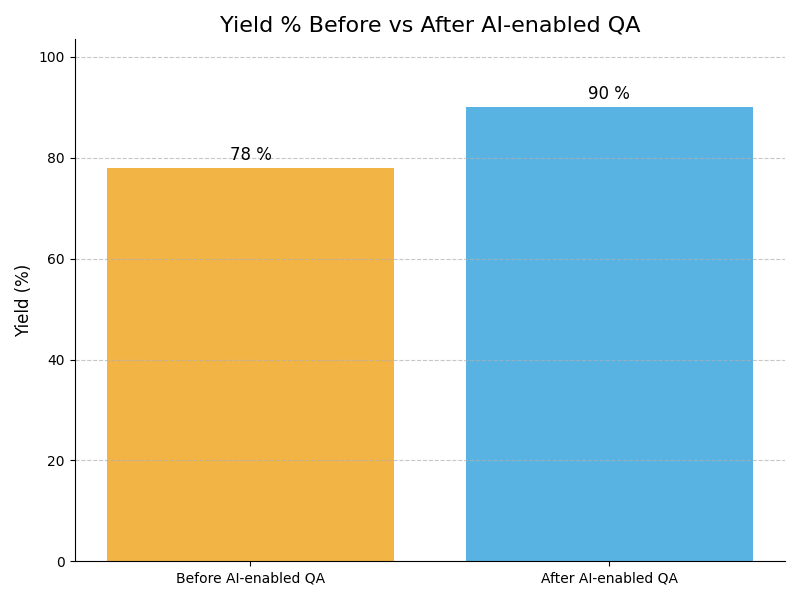
AI Wafer Scrap Reduction
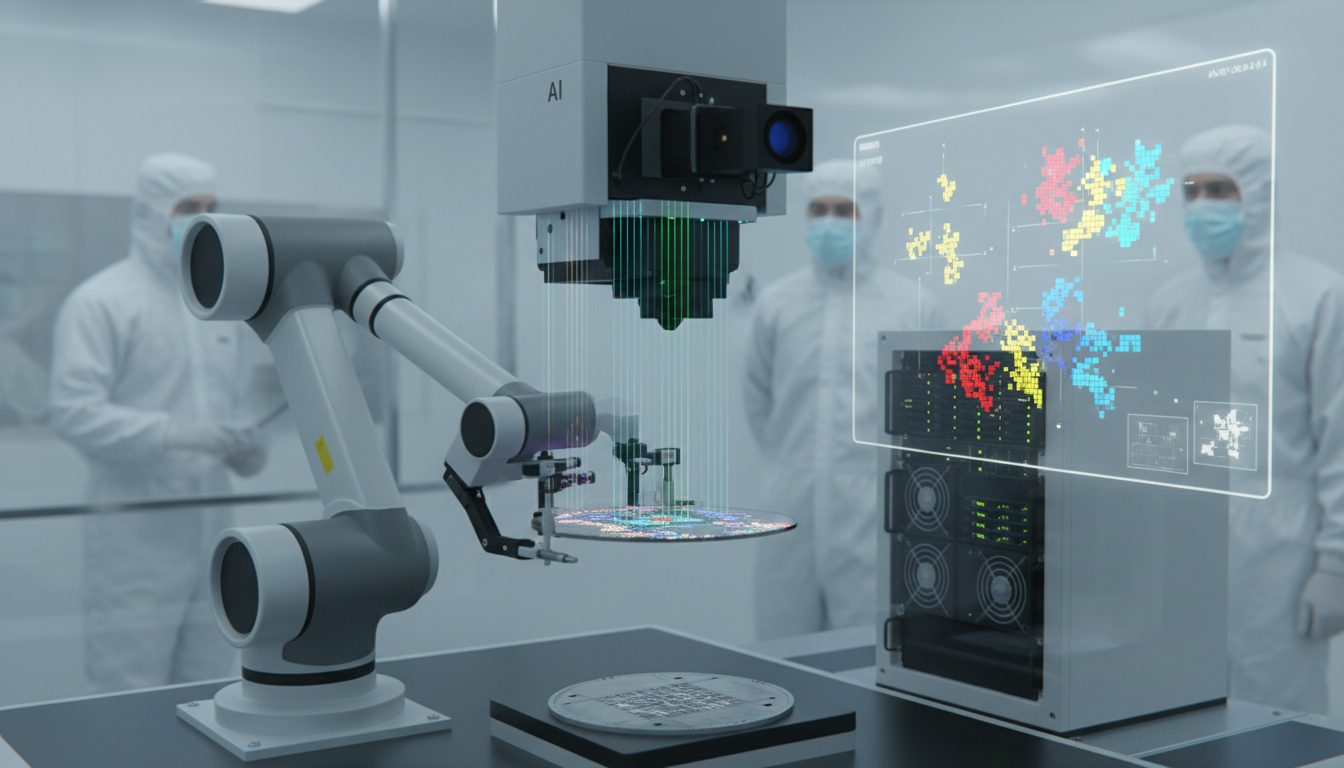
AI Wafer Scrap Reduction refers to the integration of artificial intelligence technologies in the Silicon Wafer Engineering sector, specifically aimed at minimizing material waste during the wafer manufacturing process. This approach leverages advanced algorithms and machine learning techniques to optimize production workflows, enhance yield rates, and reduce scrap. Given the increasing demand for precision and efficiency in semiconductor fabrication, this focus on scrap reduction is now more relevant than ever. It aligns with the broader trend of AI-led transformation, addressing operational inefficiencies while providing significant value to manufacturers and stakeholders alike.
The significance of the Silicon Wafer Engineering ecosystem in the context of AI Wafer Scrap Reduction cannot be overstated. AI-driven practices are fundamentally reshaping how companies compete, innovate, and interact with stakeholders, fostering a more agile and responsive environment. By harnessing AI, organizations can enhance decision-making processes, streamline operations, and establish long-term strategic objectives that prioritize sustainability. However, while the potential for growth is substantial, challenges such as adoption barriers , integration complexity, and evolving expectations must be navigated carefully to fully realize these benefits.
Maximize Efficiency: Implement AI Strategies for Wafer Scrap Reduction
Companies in the Silicon Wafer Engineering sector should strategically invest in AI technologies and forge partnerships with data-driven firms to enhance wafer scrap reduction initiatives. By leveraging AI, organizations can expect significant reductions in waste, improved yield rates, and a competitive edge in the market through operational excellence.
Transforming Silicon Wafer Engineering: The Role of AI in Scrap Reduction
Implementation Framework
Utilize AI for scrap forecasting
Set up AI-driven monitoring systems
Adjust parameters using AI insights
Educate staff on AI applications
Regularly assess AI implementation
Leverage AI-driven predictive analytics to forecast wafer scrap rates accurately, enabling proactive measures to minimize waste. This approach enhances operational efficiency and reduces costs significantly while improving supply chain resilience.
Technology Partners
Establish real-time monitoring systems powered by AI to detect anomalies and inefficiencies in wafer production . This allows for immediate corrective actions, reducing scrap and enhancing overall production quality.
Industry Standards
Utilize AI algorithms to analyze and optimize manufacturing process parameters, thereby reducing variations that lead to scrap. This results in improved yield rates and higher profitability in wafer production operations.
Internal R&D
Implement comprehensive training programs for employees on AI tools and technologies, fostering a culture of innovation and enhancing skills essential for effective scrap reduction in wafer engineering processes.
Cloud Platform
Establish a framework for continuous improvement reviews focused on AI implementation in wafer scrap reduction, facilitating adjustments based on performance metrics and ensuring alignment with evolving industry standards.
Consulting Firms
Best Practices for Automotive Manufacturers
Integrate AI Algorithms Effectively
- Impact : Enhances defect detection accuracy significantly
Example : Example: A semiconductor manufacturer implements AI algorithms to analyze real-time data from production lines, achieving a 30% increase in defect detection accuracy compared to manual inspections. - Impact : Reduces production downtime and costs
Example : Example: An electronics plant uses AI to optimize machine scheduling, significantly reducing unplanned downtime by 25% and saving thousands in operational costs. - Impact : Improves quality control standards
Example : Example: Quality control teams leverage AI-driven analytics to set thresholds for defects, leading to a 40% improvement in product compliance and customer satisfaction. - Impact : Boosts overall operational efficiency
Example : Example: Implementing AI-based predictive maintenance leads to 20% higher overall equipment efficiency, allowing the plant to meet increased demand without additional resources.
- Impact : High initial investment for implementation
Example : Example: A mid-sized semiconductor company postpones AI deployment after realizing that the cost of new sensors and training exceeds budget estimates, delaying potential benefits. - Impact : Potential data privacy concerns
Example : Example: An AI system inadvertently collects sensitive employee data, raising red flags during audit reviews and risking compliance violations. - Impact : Integration challenges with existing systems
Example : Example: A factory faces significant delays as the AI software struggles to integrate with legacy systems, causing production bottlenecks and increased labor costs. - Impact : Dependence on continuous data quality
Example : Example: An unexpected dust accumulation on AI cameras leads to misidentification of good wafers as defective, resulting in higher scrap rates until maintenance was performed.
Utilize Real-time Monitoring
- Impact : Enables proactive issue detection
Example : Example: A silicon wafer fabrication facility employs real-time monitoring systems to immediately alert operators of anomalies, allowing for swift corrective actions and reducing defect rates by 15%. - Impact : Improves response times to defects
Example : Example: With real-time data feeds, a wafer manufacturer can halt production instantly when defects are detected, leading to a 20% reduction in scrap material costs over time. - Impact : Reduces unnecessary scrap generation
Example : Example: Real-time analytics provide management with insights into production efficiency, revealing opportunities to cut waste and improve resource allocation in operations by 30%. - Impact : Enhances operational transparency
Example : Example: An advanced monitoring system tracks equipment performance, enabling early interventions that enhance transparency and accountability among production teams.
- Impact : System dependency on reliable data inputs
Example : Example: A wafer manufacturer struggles with inaccurate data inputs from outdated sensors, leading to incorrect defect assessments and increased scrap rates as operators cannot trust the system. - Impact : High complexity in system integration
Example : Example: Integration of real-time monitoring systems with existing machinery proves to be complex, resulting in unexpected downtime and project delays as engineers troubleshoot compatibility issues. - Impact : Potential resistance from workforce
Example : Example: Operators express resistance to relying on AI-driven insights, fearing job displacement and causing delays in full adoption of the monitoring technology. - Impact : Over-reliance on automation
Example : Example: A company over-relies on automated defect detection, leading to missed manual checks that could catch defects that the AI system fails to identify.
Train Workforce Regularly
- Impact : Enhances team adaptability to AI tools
Example : Example: A silicon wafer company invests in regular training sessions for employees on AI tool usage, resulting in a 25% increase in operational efficiency as teams become more adept at leveraging technology. - Impact : Improves operational efficiency and confidence
Example : Example: By fostering a culture of continuous learning, an organization sees a decrease in human errors during AI operations, leading to fewer misclassifications and reduced scrap rates. - Impact : Fosters a culture of continuous improvement
Example : Example: Regular training sessions enhance workforce adaptability, allowing teams to respond quickly to new AI features and updates, which improves overall productivity by 20%. - Impact : Reduces errors in AI usage
Example : Example: Employees trained to understand AI insights better can make informed decisions, leading to an overall reduction in operational errors and improved product quality.
- Impact : Training costs may exceed budget limits
Example : Example: A silicon wafer manufacturer faces budget constraints as training costs escalate, limiting the number of employees who can receive vital AI training and slowing implementation. - Impact : Time investment may disrupt production schedules
Example : Example: Employees struggle to balance training sessions with their regular duties, leading to production delays and frustration as teams become torn between responsibilities. - Impact : Potential knowledge retention issues
Example : Example: A company finds that retaining knowledge from training sessions is challenging, resulting in poor application of AI tools and a negative impact on defect reduction efforts. - Impact : Reluctance to adopt new methodologies
Example : Example: Some staff members resist adopting new methodologies taught in training, preferring traditional methods, which hinders overall progress in implementing AI solutions.
Leverage Data Analytics
- Impact : Identifies trends in wafer defects
Example : Example: A data analytics platform reveals recurring defects in specific wafer batches, allowing engineers to adjust parameters that lead to a 30% reduction in defective products. - Impact : Optimizes production processes effectively
Example : Example: By analyzing production data, a company optimizes its processes, resulting in a 25% increase in overall efficiency and reduced cycle times across fabrication lines. - Impact : Facilitates data-driven decision making
Example : Example: Data-driven insights allow management to make informed decisions on resource allocation, increasing yield rates by 15% while maintaining product quality. - Impact : Enhances yield rates significantly
Example : Example: A semiconductor firm leverages analytics to identify underperforming machines, leading to targeted improvements that enhance yield rates significantly and reduce costs.
- Impact : Data security risks during analysis
Example : Example: A semiconductor company faces a data breach during analytics processing, risking sensitive information and leading to costly legal repercussions as they rectify the situation. - Impact : Challenges in data interpretation
Example : Example: Data analysts struggle to interpret complex datasets, leading to misinformed decisions that cause production inefficiencies and increased scrap rates. - Impact : Dependence on data accuracy
Example : Example: A new AI system fails to function correctly due to inaccurate data inputs, causing unexpected downtime and lost production time while engineers troubleshoot the issues. - Impact : Integration issues with AI systems
Example : Example: Integration between data analytics tools and existing AI systems proves complicated, delaying insights and hampering the overall efficiency of production processes.
Implement Predictive Maintenance
- Impact : Minimizes unexpected equipment failures
Example : Example: A silicon wafer manufacturer adopts predictive maintenance, resulting in a 40% reduction in unexpected equipment failures, ensuring smoother production flows and increased uptime. - Impact : Reduces maintenance costs significantly
Example : Example: By implementing AI-driven predictive maintenance, costs associated with routine repairs decrease by 30%, freeing up resources for other operational improvements. - Impact : Extends equipment lifespan
Example : Example: Predictive maintenance technologies enable a company to extend the lifespan of critical machinery, resulting in significant long-term savings and better ROI on equipment investments. - Impact : Enhances production consistency
Example : Example: Enhanced equipment consistency leads to fewer production disruptions, resulting in improved output quality and a reduction in scrap rates by 20%.
- Impact : Initial setup costs may be high
Example : Example: A semiconductor facility faces challenges with high initial costs for implementing predictive maintenance systems, causing delays in overall operational improvements and budget constraints. - Impact : Requires skilled personnel for implementation
Example : Example: The company struggles to find skilled personnel to operate and maintain predictive systems, leading to extended downtime and inefficiencies in production processes. - Impact : Risk of overfitting predictive models
Example : Example: A predictive model becomes overfitted to historical data, failing to adapt to new conditions and leading to inaccurate maintenance predictions and increased equipment failures. - Impact : Dependence on historical data quality
Example : Example: If the historical data used for predictive maintenance is of poor quality, it can result in misleading analyses, undermining the system's effectiveness and increasing scrap rates.
Establish Cross-functional Teams
- Impact : Fosters collaboration across departments
Example : Example: A silicon wafer plant forms cross-functional teams that bring together engineers, data scientists, and operators. This collaboration fosters innovative solutions that reduce scrap rates by 15%. - Impact : Encourages knowledge sharing and innovation
Example : Example: Regular meetings among cross-functional teams encourage knowledge sharing, allowing teams to leverage insights that lead to enhanced production strategies and improved operational efficiencies. - Impact : Improves problem-solving capabilities
Example : Example: Problem-solving capabilities improve as diverse teams tackle challenges, resulting in faster resolution of defects and a noticeable decrease in overall scrap production. - Impact : Aligns AI strategy with business goals
Example : Example: Aligning AI initiatives with business goals through cross-functional teamwork leads to more strategic investments and a robust return on investment, enhancing overall competitiveness.
- Impact : Potential for communication breakdowns
Example : Example: A silicon wafer manufacturer experiences communication breakdowns between teams, leading to misunderstandings about AI project goals and delays in implementation timelines. - Impact : Resource allocation may be challenging
Example : Example: Cross-functional teams struggle with allocating resources effectively, causing project delays as team members are pulled into conflicting priorities across departments. - Impact : Conflicting departmental priorities
Example : Example: Conflicting priorities between engineering and production teams create friction, leading to stalled projects and a lack of alignment on AI strategy and objectives. - Impact : Increased meeting times may hinder productivity
Example : Example: Increased meeting times for cross-functional collaboration can hinder productivity, as employees find it challenging to balance project work with necessary discussions.
AI is revolutionizing semiconductor manufacturing by enabling the production of the most advanced AI chips on US soil for the first time, significantly reducing dependency on foreign wafers and minimizing production scrap through domestic reindustrialization.
– Jensen Huang, CEO of NvidiaCompliance Case Studies
Seize the opportunity to enhance efficiency and cut costs with AI-driven solutions. Transform your operations and stay ahead in Silicon Wafer Engineering .
Take Test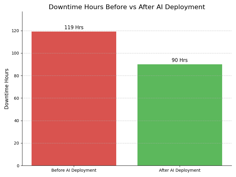
Leadership Challenges & Opportunities
Data Quality Management
Implement AI Wafer Scrap Reduction to enhance data analytics and ensure high-quality input for decision-making processes. Utilize real-time data validation and cleansing tools to minimize errors in wafer fabrication data, leading to more precise scrap reduction strategies and improved overall yield.
Cultural Resistance to Change
Foster a culture of innovation by integrating AI Wafer Scrap Reduction into existing workflows incrementally. Engage teams through workshops and success stories to demonstrate quick wins, while providing continuous feedback loops to facilitate acceptance and collaboration in adopting new technologies.
High Implementation Costs
Utilize AI Wafer Scrap Reduction through modular deployment strategies that allow for phased integration without significant upfront investment. Focus on critical areas with immediate ROI, and leverage cloud-based solutions to spread costs over time, ensuring sustainable financial impacts on operations.
Skill Deficiencies in AI
Address skill gaps by offering targeted training programs focused on AI Wafer Scrap Reduction tools and techniques. Collaborate with educational institutions for upskilling initiatives and incorporate AI mentorship programs within the organization to build a knowledgeable workforce capable of driving innovation.
Assess how well your AI initiatives align with your business goals
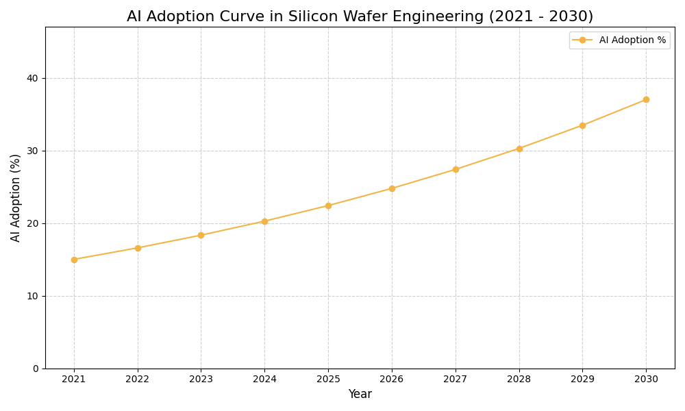
AI Adoption Graph
AI Use Case vs ROI Timeline
| AI Use Case | Description | Typical ROI Timeline | Expected ROI Impact |
|---|---|---|---|
| Predictive Maintenance for Equipment | AI algorithms analyze equipment performance data to predict failures before they occur. For example, implementing predictive maintenance on etching machines reduces unexpected downtimes and scrap rates significantly, ensuring better operation efficiency. | 6-12 months | High |
| Process Optimization Algorithms | AI-driven analytics optimize manufacturing processes to minimize scrap. For example, using AI to adjust parameters in photolithography can lead to an immediate reduction in wafer defects and material waste. | 12-18 months | Medium-High |
| Quality Control Automation | AI systems enhance quality control by analyzing wafer quality data in real-time. For example, integrating machine vision to inspect wafers during production can detect defects early, reducing scrap and rework. | 6-12 months | High |
| Supply Chain Optimization | AI improves supply chain logistics to ensure timely material availability, reducing excess inventory and waste. For example, using AI to predict demand fluctuations helps maintain optimal wafer production levels, minimizing scrap. | 12-18 months | Medium-High |
Glossary
Work with Atomic Loops to architect your AI implementation roadmap — from PoC to enterprise scale.
Contact NowFrequently Asked Questions
- AI Wafer Scrap Reduction minimizes waste through intelligent data-driven decision-making processes.
- It improves yield rates by identifying and addressing inefficiencies in wafer production.
- Companies benefit from enhanced resource allocation and reduced operational costs.
- The technology fosters innovation by enabling rapid adjustments based on real-time analytics.
- Ultimately, it contributes to a more sustainable and profitable manufacturing environment.
- Begin with a thorough assessment of current processes and technology infrastructure.
- Identify key stakeholders and create a cross-functional team for project execution.
- Pilot small-scale AI solutions to test feasibility and gather insights before full deployment.
- Invest in training programs to upskill teams on AI technologies and their applications.
- Establish clear objectives and metrics to measure success throughout the implementation phase.
- Organizations often see improved yield rates, leading to higher production efficiency.
- Cost reductions result from decreased material waste and optimized processes.
- AI facilitates faster decision-making, allowing companies to respond swiftly to market changes.
- Enhanced product quality directly correlates to increased customer satisfaction and loyalty.
- Companies gain a competitive edge by leveraging innovative technologies for continuous improvement.
- Resistance to change can hinder adoption; effective change management strategies are essential.
- Data quality issues may affect AI performance, necessitating rigorous data cleaning processes.
- Integration complexities with legacy systems require careful planning and resource allocation.
- Skill gaps in the workforce can limit successful implementation; invest in training and development.
- Regulatory compliance must be considered to avoid potential legal and operational pitfalls.
- Start with clear objectives to align AI initiatives with business goals and strategies.
- Engage stakeholders early and often to foster buy-in and collaborative efforts.
- Utilize a phased implementation approach to manage risks and demonstrate quick wins.
- Regularly review and adjust AI models based on performance metrics and industry standards.
- Stay informed about emerging technologies and trends to continuously enhance AI capabilities.
- Compliance with industry standards ensures operational integrity and product quality.
- AI technologies should be evaluated for adherence to relevant regulatory frameworks.
- Understanding compliance requirements helps mitigate risks during the implementation process.
- Regular audits and assessments can maintain alignment with evolving industry benchmarks.
- Collaboration with regulatory bodies may enhance trust and facilitate smoother operations.