
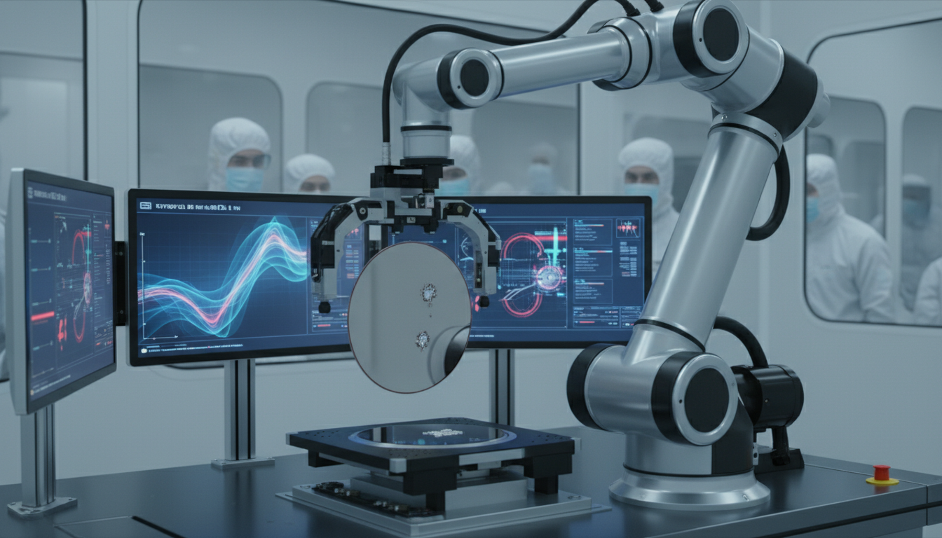
AI Wafer Layout Optimize
AI Wafer Layout Optimize refers to the application of artificial intelligence techniques to enhance the design and layout of silicon wafer s in semiconductor manufacturing. This process involves leveraging advanced algorithms to predict optimal configurations, thereby maximizing yield and performance . It is increasingly relevant as semiconductor companies strive to meet the demands of more complex and efficient chip designs, aligning with the broader trends of AI-led transformation across technology sectors.
The Silicon Wafer Engineering ecosystem is experiencing profound changes driven by AI methodologies, which are redefining competitive landscapes and innovation cycles. As stakeholders engage with AI practices, they witness improvements in operational efficiency and decision-making processes. This shift not only opens avenues for growth but also presents challenges such as integration complexities and evolving expectations from clients and partners. Balancing the transformative potential of AI with these challenges will be crucial for stakeholders aiming to thrive in a rapidly evolving environment.
Maximize Efficiency with AI Wafer Layout Optimization
Silicon Wafer Engineering firms should strategically invest in partnerships with AI technology providers to enhance wafer layout optimization processes. Implementing these AI-driven strategies is expected to yield significant improvements in production efficiency, cost reduction, and a competitive edge in the market.
How AI is Revolutionizing Wafer Layout Optimization?
Implementation Framework
Utilize advanced algorithms for optimization
Incorporate ML for predictive analytics
Visualize data for better insights
Test layouts iteratively for improvements
Facilitate teamwork with AI tools
Implement AI algorithms for wafer layout optimization to enhance design efficiency, reduce material waste, and improve yield rates. This step ensures competitive advantage through enhanced precision and minimized errors in designs.
Technology Partners
Integrate machine learning techniques to analyze historical data and predict optimal wafer layouts. This data-driven approach enhances decision-making and aligns with supply chain resilience, adapting to market demands effectively.
Industry Standards
Deploy data visualization tools to present complex design data clearly. Enhanced visualization aids engineers in understanding layout decisions, fostering collaboration, and driving informed choices that optimize wafer performance and efficiency.
Internal R&D
Establish iterative testing protocols for wafer layouts using AI simulations. Continuous testing enables rapid identification of design flaws and allows for quick adjustments, ultimately improving yield and reducing costs in wafer production .
Cloud Platform
Adopt collaborative platforms that utilize AI for project management and design reviews. These tools enhance communication among teams, streamline workflows, and ensure that AI insights are effectively shared, maximizing project outcomes.
Technology Partners
Best Practices for Automotive Manufacturers
Leverage Predictive Analytics Techniques
- Impact : Increases yield prediction accuracy
Example : Example: A semiconductor fab implemented predictive analytics to forecast yield, resulting in a 20% increase in production efficiency by identifying potential yield issues before they occurred. - Impact : Reduces scrap rate effectively
Example : Example: An electronics manufacturer used AI to analyze historical data, reducing scrap rates by 15% by optimizing wafer layouts based on past performance insights. - Impact : Facilitates proactive maintenance scheduling
Example : Example: A wafer fabrication facility employed AI-driven scheduling to predict maintenance needs, which led to a 30% reduction in unplanned downtime, improving overall productivity significantly. - Impact : Enhances resource allocation efficiency
Example : Example: By utilizing AI for resource allocation, a silicon wafer plant reduced material wastage by 25%, ensuring better utilization of raw materials and cost savings.
- Impact : Requires advanced data integration skills
Example : Example: A leading wafer manufacturer faced integration issues when trying to implement AI tools, leading to delays and increased costs due to a lack of skilled personnel for data integration. - Impact : Potential over-reliance on automated systems
Example : Example: A company became overly reliant on its AI for layout optimization, which led to missed opportunities for human insight that could have improved final outcomes, resulting in lower-quality products. - Impact : Challenges in data quality management
Example : Example: An AI system used for wafer inspection misidentified defects due to poor data quality, leading to significant production errors until data management practices were improved. - Impact : Risk of algorithmic bias in decisions
Example : Example: A silicon wafer producer faced backlash after its AI system favored certain layout designs, inadvertently introducing biases that affected product diversity and market reach.
Integrate AI Algorithms Effectively
- Impact : Enhances defect detection accuracy significantly
Example : Example: In an automotive assembly line, a vision-based AI system flags microscopic paint defects in real time as car bodies pass under cameras, catching flaws human inspectors previously missed during night shifts. - Impact : Reduces production downtime and costs
Example : Example: A semiconductor factory uses AI to detect early soldering anomalies. The system stops the line immediately, preventing a full batch failure that would have caused hours of rework and shutdown. - Impact : Improves quality control standards
Example : Example: A food packaging plant uses AI image recognition to verify seal integrity on every packet, ensuring non-compliant packages are rejected instantly before shipping. - Impact : Boosts overall operational efficiency
Example : Example: AI dynamically adjusts inspection thresholds based on production speed, allowing the factory to increase output during peak demand without sacrificing quality.
- Impact : High initial investment for implementation
Example : Example: A mid-sized electronics manufacturer delays AI rollout after realizing camera hardware, GPUs, and system integration push upfront costs beyond budget approvals. - Impact : Potential data privacy concerns
Example : Example: AI quality systems capturing worker activity unintentionally store employee facial data, triggering compliance issues with internal privacy policies. - Impact : Integration challenges with existing systems
Example : Example: AI software cannot communicate with a 15-year-old PLC controller, forcing engineers to manually export data and slowing decision-making. - Impact : Dependence on continuous data quality
Example : Example: Dust accumulation on camera lenses causes the AI to misclassify normal products as defective, leading to unnecessary scrap until recalibration.
Utilize Real-time Monitoring Systems
- Impact : Improves decision-making speed
Example : Example: A silicon wafer manufacturer implemented real-time monitoring, which allowed engineers to make informed decisions on the fly, enhancing responsiveness during production processes by 25%. - Impact : Enables immediate corrective actions
Example : Example: By utilizing AI-driven monitoring, a fab was able to identify and rectify production anomalies within minutes, significantly reducing the time to implement corrective actions. - Impact : Enhances operational transparency
Example : Example: An electronics plant improved operational transparency through real-time data display, enabling better communication among teams and resulting in a cohesive approach to quality control. - Impact : Facilitates performance benchmarking
Example : Example: The introduction of AI monitoring facilitated performance benchmarking across different production lines, revealing best practices that improved overall factory output by 18%.
- Impact : High infrastructure costs for data collection
Example : Example: A semiconductor facility faced challenges when implementing AI monitoring due to high infrastructure costs, resulting in budget overruns that delayed the project timeline. - Impact : Potential for false alarms disrupting processes
Example : Example: A fab encountered frequent false alarms from their AI system, which disrupted normal operations and led to unnecessary downtime until algorithms were refined. - Impact : Need for continuous system updates
Example : Example: An electronics manufacturer struggled with the need for continuous updates to their AI monitoring system, causing inconsistent performance and reliability issues over time. - Impact : Dependency on reliable internet connectivity
Example : Example: A silicon wafer plant's reliance on internet connectivity for real-time monitoring led to significant operational disruptions during network outages, affecting production schedules.
Optimize Training for AI Usage
- Impact : Enhances employee skill sets
Example : Example: A silicon wafer facility implemented a comprehensive AI training program, resulting in a 40% increase in employee proficiency and confidence in using AI tools effectively. - Impact : Promotes seamless technology adoption
Example : Example: By providing targeted AI training sessions, a fab ensured smooth technology adoption, leading to a 30% reduction in initial operational hiccups during implementation. - Impact : Reduces resistance to change
Example : Example: A company experienced less resistance to change after conducting workshops that highlighted AI benefits, fostering a culture of innovation and adaptability among employees. - Impact : Improves collaboration across teams
Example : Example: Collaboration improved significantly in a semiconductor plant after training employees on AI tools, leading to better communication and problem-solving across various departments.
- Impact : Training costs can be substantial
Example : Example: A semiconductor manufacturer faced high training costs that exceeded initial budgets, leading to cuts in other operational areas due to resource allocation issues. - Impact : Learning curve may hinder productivity
Example : Example: A company experienced a temporary drop in productivity as employees navigated the learning curve associated with new AI tools , which slowed down production for a critical period. - Impact : Inconsistent training quality may arise
Example : Example: A fab struggled with inconsistent training quality as different trainers presented varied approaches, leading to confusion and inefficiencies among staff using AI tools. - Impact : Potential for knowledge silos to develop
Example : Example: Knowledge silos emerged in a silicon wafer facility when only certain teams received specialized AI training, hindering overall collaboration and innovation across departments.
Engage Stakeholders in AI Projects
- Impact : Increases project buy-in from teams
Example : Example: When launching an AI project, a semiconductor manufacturer involved cross-functional teams from the start, leading to improved buy-in and a smoother implementation process. - Impact : Facilitates better resource allocation
Example : Example: By engaging stakeholders early in the AI development phase, a fab was able to secure better resource allocation, ensuring project success from the outset. - Impact : Enhances communication across departments
Example : Example: Communication improved significantly across departments in a silicon wafer factory after stakeholder engagement sessions, resulting in coordinated efforts towards common AI goals. - Impact : Aligns goals with organizational strategy
Example : Example: A company aligned its AI initiatives with overall organizational strategy by involving senior leadership in discussions, ensuring that projects were relevant and impactful.
- Impact : Stakeholder conflicts may arise
Example : Example: A silicon wafer manufacturer faced conflicts among stakeholders over project priorities, causing delays and frustration that impacted the rollout of AI initiatives. - Impact : Project scope can expand uncontrollably
Example : Example: An electronics firm encountered scope creep in their AI project due to varying stakeholder inputs, leading to budget overruns and timeline extensions. - Impact : Diverse expectations can complicate processes
Example : Example: Diverse expectations from different teams complicated the AI implementation process, causing confusion and miscommunication that delayed project milestones. - Impact : Dependency on stakeholder availability
Example : Example: A semiconductor facility's reliance on stakeholders for project decisions led to delays when key individuals became unavailable, stalling progress on critical AI initiatives.
Conduct Regular System Evaluations
- Impact : Identifies areas for improvement
Example : Example: A silicon wafer fab established a routine evaluation process for its AI systems, which revealed performance gaps, leading to targeted improvements and a 15% efficiency boost. - Impact : Informs future AI strategy
Example : Example: By conducting regular evaluations, a semiconductor manufacturer informed its future AI strategy , ensuring alignment with evolving market demands and technology advancements. - Impact : Enhances system reliability
Example : Example: A company improved its system reliability by instituting regular evaluations, decreasing system failures and downtime, thus enhancing overall productivity. - Impact : Boosts user satisfaction levels
Example : Example: User satisfaction increased in a silicon wafer facility as a result of regular evaluations that addressed employee feedback, ensuring AI tools met their operational needs effectively.
- Impact : Time-consuming evaluation processes
Example : Example: A semiconductor manufacturer found that their evaluation process was time-consuming, leading to delays in implementing necessary system updates and improvements. - Impact : Potential for bias in evaluations
Example : Example: Biases in the evaluation team led to skewed results that did not accurately depict AI system performance, resulting in misaligned improvement strategies. - Impact : Inconsistent evaluation criteria may arise
Example : Example: A fab struggled with inconsistent evaluation criteria, leading to confusion over performance standards and making it difficult to track improvement progress over time. - Impact : Risk of overlooking critical issues
Example : Example: In a silicon wafer facility , critical issues were overlooked during evaluations due to a focus on surface-level metrics, preventing meaningful enhancements from being made.
We manufactured the most advanced AI chips in the world, in the most advanced fab in the United States for the first time, marking the beginning of AI-driven wafer production revolutionizing semiconductor layout and manufacturing.
– Jensen Huang, CEO of NvidiaCompliance Case Studies


Transform your silicon wafer layouts with AI-driven optimization. Gain a competitive edge and unlock unprecedented efficiency in your engineering processes. Don’t get left behind!
Take Test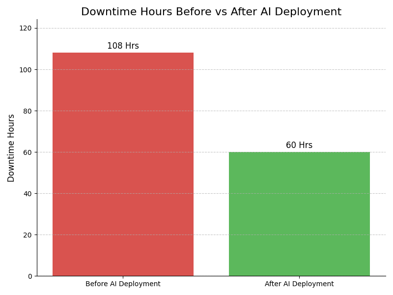
Leadership Challenges & Opportunities
Data Integration Challenges
Utilize AI Wafer Layout Optimize to automate data integration from various sources, ensuring consistent and accurate layout data. Implement machine learning algorithms to enhance data correlation and reduce errors. This streamlines the design process, enhances precision, and accelerates time-to-market for new wafers.
Cultural Resistance to Change
Foster a culture of innovation by demonstrating the benefits of AI Wafer Layout Optimize through pilot projects. Engage stakeholders with workshops to showcase its impact on efficiency and quality. This approach promotes acceptance and encourages a mindset shift towards embracing advanced technologies within the organization.
High Implementation Costs
Leverage AI Wafer Layout Optimize’s modular architecture to implement in phases, focusing on high-impact areas first. Identify cost-effective cloud solutions that reduce upfront investments. This strategy allows for incremental ROI assessment, ensuring financial viability and resource allocation for broader implementation over time.
Talent Acquisition Issues
Enhance recruitment and retention strategies by partnering with academic institutions to cultivate a talent pipeline skilled in AI and wafer engineering. Implement training programs using AI Wafer Layout Optimize that provide employees with hands-on experience, ensuring that the workforce is prepared to leverage advanced technologies effectively.
Assess how well your AI initiatives align with your business goals
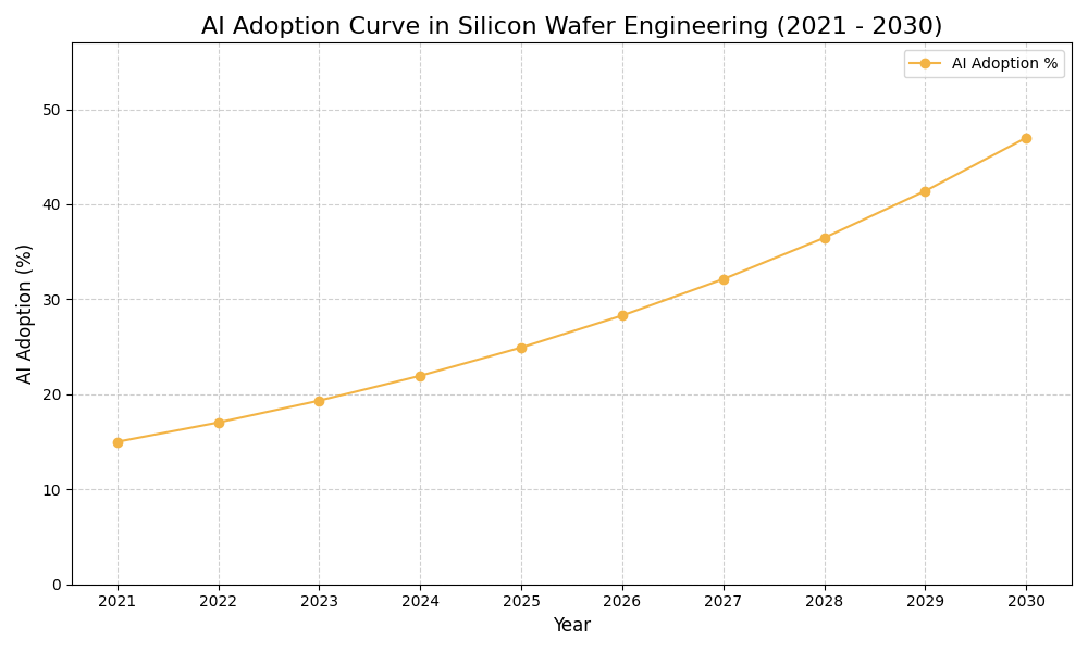
AI Adoption Graph
AI Use Case vs ROI Timeline
| AI Use Case | Description | Typical ROI Timeline | Expected ROI Impact |
|---|---|---|---|
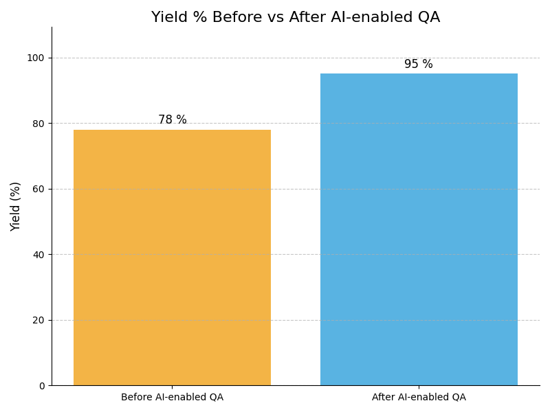
| Yield Optimization through Layout Analysis | AI algorithms analyze wafer layouts to identify optimal configurations, enhancing yield rates. For example, a semiconductor manufacturer increased yield by 15% by adjusting die placements based on AI predictions. | 6-12 months | High |
| Defect Prediction with Machine Learning | Implementing AI to predict potential defects in wafer layouts, enabling preemptive adjustments. For example, a company reduced defects by 20% by analyzing past layout data to forecast issues. | 12-18 months | Medium-High |
| Cost Reduction via Resource Allocation | AI optimizes the allocation of resources in the fabrication process, reducing material waste. For example, a fab facility minimized costs by 10% through smarter resource management based on AI analytics. | 6-12 months | Medium |
| Process Efficiency Enhancement | Using AI to streamline the wafer fabrication process by optimizing layout designs. For example, a manufacturer improved processing time by 25% by implementing AI-driven layout simulations. | 6-12 months | High |
Glossary
Work with Atomic Loops to architect your AI implementation roadmap — from PoC to enterprise scale.
Contact NowFrequently Asked Questions
- AI Wafer Layout Optimize uses advanced algorithms to enhance wafer layout efficiency.
- It significantly reduces design errors and improves yield rates through intelligent analysis.
- The technology enables faster time-to-market for new semiconductor products.
- Companies can achieve better resource allocation and operational cost savings.
- This optimization leads to improved product quality and competitive advantage.
- Begin with a needs assessment to identify specific challenges and goals.
- Engage stakeholders to ensure alignment with business objectives and requirements.
- Consider pilot programs to test AI integration on a smaller scale first.
- Invest in training for staff to ensure they can effectively use the new tools.
- Collaborate with AI solution providers for tailored implementation strategies.
- Organizations can see improvements in yield rates due to optimized layouts.
- Reduced design iterations lead to faster project completion times.
- Companies often report lower operational costs through enhanced efficiencies.
- Quality metrics improve as errors decrease in the layout process.
- Data-driven insights enable better decision-making and strategic planning.
- Data quality issues can hinder the effectiveness of AI algorithms in layouts.
- Resistance to change from staff can slow down the implementation process.
- Integration challenges with existing systems may arise during deployment.
- Lack of clear objectives can lead to misalignment and wasted resources.
- Ongoing maintenance and updates are necessary to sustain AI performance.
- Investing in AI can lead to significant cost savings over time through efficiency gains.
- Companies gain a competitive edge by reducing time-to-market for new products.
- AI-driven analysis enhances decision-making and operational accuracy.
- Improved yield rates translate to higher profitability for semiconductor manufacturers.
- Such technology supports innovation by enabling complex designs at scale.
- Organizations should consider adoption when facing significant design challenges.
- Timing is critical if market competition is increasing and innovation is needed.
- When there's a clear demand for faster product development, adoption is beneficial.
- Evaluate readiness based on existing digital infrastructure and capabilities.
- Early adoption can set the stage for long-term competitive advantages.
- Benchmarks often include yield rate improvements and reduced design cycle times.
- Compliance with industry standards can guide successful AI implementations.
- Evaluating peer adoption rates can provide insights into best practices.
- Success metrics should align with organizational goals and market demands.
- Continuous monitoring against these benchmarks ensures ongoing improvement.