AI Vision Crack Detection
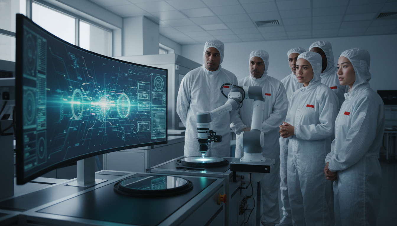
AI Vision Crack Detection refers to the integration of artificial intelligence technologies in identifying and analyzing cracks in silicon wafer s, which are crucial components in the semiconductor manufacturing process. This innovative approach utilizes advanced imaging and machine learning algorithms to enhance defect detection, ensuring higher quality and reliability in production. As the demand for precision in the semiconductor field intensifies, the relevance of AI Vision Crack Detection becomes paramount, aligning with the broader shift towards AI-driven operational excellence and strategic agility .
In the realm of Silicon Wafer Engineering , the adoption of AI Vision Crack Detection is not just a technological upgrade but a catalyst for transformative change. It reshapes how stakeholders interact, driving innovation cycles and competitive differentiation. By leveraging AI, organizations can significantly improve efficiency and decision-making processes, paving the way for long-term strategic advantages. However, while the growth potential is substantial, challenges such as integration complexity and evolving stakeholder expectations must be addressed to fully realize the benefits of this technological shift.
Unlock Competitive Advantages with AI Vision Crack Detection
Silicon Wafer Engineering companies should strategically invest in partnerships focused on AI Vision Crack Detection technology to enhance quality assurance processes. Implementing these AI-driven solutions is expected to yield substantial ROI through reduced defect rates, increased throughput, and strengthened market position.
How AI Vision Crack Detection is Revolutionizing Silicon Wafer Engineering
Implementation Framework
Create frameworks for data collection and analysis
Deploy machine learning models for analysis
Enhance skills for AI integration
Track AI efficiency and outcomes
Refine processes based on insights
Develop robust data protocols to ensure high-quality, structured data capture for AI algorithms. This enhances the effectiveness of crack detection while reducing false positives, thus improving operational efficiency.
Internal R&D
Integrate advanced machine learning algorithms that analyze data in real-time, enhancing the detection of cracks in silicon wafers. This leads to reduced downtime and improved product quality through automated inspections.
Technology Partners
Provide comprehensive training programs for employees to effectively utilize AI tools, ensuring a smoother transition to automated crack detection systems. This fosters a culture of innovation and boosts productivity across teams.
Industry Standards
Establish key performance indicators (KPIs) to continuously monitor the effectiveness of AI in crack detection. This allows for proactive adjustments and optimizations, ensuring sustained operational excellence in silicon wafer production .
Cloud Platform
Continuously evaluate and refine AI processes based on performance data, fostering an agile environment that adapts to new insights for improved crack detection accuracy and operational resilience in wafer engineering .
Internal R&D
Best Practices for Automotive Manufacturers
Implement Real-time Monitoring Systems
- Impact : Enhances defect detection accuracy significantly
Example : Example: A silicon wafer manufacturer deploys real-time monitoring, detecting cracks as they form during processing. This allows for immediate corrective action, reducing defects and improving overall yield by 15%. - Impact : Enables immediate response to quality issues
Example : Example: A fab facility integrates live AI monitoring, catching critical flaws in substrate layers. This swift detection prevents costly production halts, saving the company approximately $200,000 annually in downtime. - Impact : Reduces production downtime and costs
Example : Example: A semiconductor plant leverages AI to monitor wafer quality in real-time, ensuring that defects are flagged immediately. This proactive approach elevates the quality assurance process, enhancing customer satisfaction. - Impact : Boosts operational transparency and trust
Example : Example: By using AI-driven monitoring, a wafer processing unit identifies anomalies in real-time, enabling staff to address issues promptly, which enhances operational transparency and builds stakeholder trust.
- Impact : High initial investment for implementation
Example : Example: A silicon wafer company hesitates to implement AI due to the daunting costs of upgrading equipment and software, leading to delays in enhancing their inspection processes. - Impact : Potential data privacy concerns
Example : Example: Employees express concerns about AI systems capturing sensitive data, which could lead to potential breaches of compliance regulations, creating friction in workplace trust. - Impact : Integration challenges with existing systems
Example : Example: A manufacturer finds their new AI system struggles to integrate with legacy machinery, causing a slowdown in production and requiring additional resources for troubleshooting. - Impact : Dependence on continuous data quality
Example : Example: An AI inspection system fails to operate effectively due to inconsistent data inputs from aging sensors, leading to misclassifications and increased waste until the sensors are replaced.
Train Workforce on AI Utilization
- Impact : Improves employee engagement with technology
Example : Example: A silicon wafer facility conducts comprehensive AI training for technicians. This initiative improves their engagement with the technology, resulting in a 25% increase in productivity as they become more adept at using AI tools. - Impact : Boosts overall productivity and morale
Example : Example: By providing regular AI utilization workshops, a semiconductor company sees a marked rise in employee morale. Workers feel more empowered and are better equipped to handle AI-driven processes effectively. - Impact : Enhances AI system effectiveness and reliability
Example : Example: A fab lab introduces AI training programs, leading to a smoother adoption of new technologies. This results in a 30% decrease in operational errors, showcasing the importance of proper training. - Impact : Reduces resistance to technological change
Example : Example: A wafer engineering firm invests in ongoing AI education, reducing resistance to change among staff. This proactive approach leads to a seamless transition towards automated quality inspections.
- Impact : Underestimating training time requirements
Example : Example: A silicon wafer manufacturer underestimates the time required for comprehensive employee training, leading to delays in AI implementation and operational inefficiencies that cost time and resources. - Impact : Potential employee pushback against AI
Example : Example: Employees in a semiconductor plant resist AI technology due to fear of job loss, resulting in a lack of cooperation and undermining the system's potential benefits during the initial rollout phase. - Impact : Skill gaps in the existing workforce
Example : Example: A company discovers significant skill gaps in its workforce, which delays the effective use of AI systems and increases reliance on external consultants, driving up costs significantly. - Impact : Difficulty in measuring training effectiveness
Example : Example: A wafer fabrication unit struggles to measure the effectiveness of its AI training program, making it difficult to justify ongoing investments and refine educational strategies for future training.
Leverage Predictive Analytics
- Impact : Anticipates equipment failures before they occur
Example : Example: A silicon wafer producer uses predictive analytics to foresee equipment failures, allowing for timely interventions. This proactive maintenance reduces unplanned downtimes by 20%, significantly enhancing production schedules. - Impact : Optimizes maintenance schedules and costs
Example : Example: By implementing AI-driven predictive analytics, a semiconductor company optimizes its maintenance schedules, reducing costs by 15% while ensuring machinery operates at peak performance without interruptions. - Impact : Improves overall production efficiency
Example : Example: A fab lab utilizes AI to analyze production data, identifying inefficiencies and adjusting processes dynamically. This boosts overall production efficiency by 18%, facilitating a smoother workflow. - Impact : Reduces scrap rates and waste
Example : Example: A wafer engineering firm relies on AI to predict potential defects during production runs. By doing so, it reduces scrap rates by 12%, leading to more sustainable operations and cost savings.
- Impact : Inaccurate predictions leading to failures
Example : Example: A semiconductor manufacturer faced production delays due to inaccurate predictions by their AI system, leading to unexpected equipment failures that negatively impacted their output. - Impact : Dependence on historical data quality
Example : Example: A silicon wafer company discovers that outdated historical data hampers accurate predictions, resulting in maintenance schedules that fail to address actual equipment conditions, causing unexpected downtimes. - Impact : Integration complexity with legacy systems
Example : Example: A fab facility struggles to integrate predictive analytics with their existing legacy systems, complicating data flow and hindering effective decision-making across departments. - Impact : Overreliance on technology for decision-making
Example : Example: An engineering firm becomes overly reliant on AI for operational decisions, neglecting critical human oversight. This results in missed opportunities for improvement and a decline in overall operational effectiveness.
Adopt Continuous Improvement Practices
- Impact : Fosters a culture of innovation
Example : Example: A silicon wafer company embraces continuous improvement practices, encouraging employees to propose innovations. This culture leads to the development of a new inspection method that increases efficiency by 30%. - Impact : Enhances adaptability to market changes
Example : Example: By adopting continuous improvement methodologies, a semiconductor firm quickly adapts to market demands, allowing for faster product launches and a 20% increase in market share. - Impact : Promotes long-term sustainability
Example : Example: A wafer engineering company regularly reviews processes for enhancements, driving long-term sustainability. This approach leads to a significant reduction in resource consumption and waste over time. - Impact : Improves competitive positioning
Example : Example: Implementing a continuous improvement strategy enables a fab lab to stay ahead of competitors by rapidly adapting processes, resulting in improved customer satisfaction and loyalty.
- Impact : Resistance to change from employees
Example : Example: A silicon wafer manufacturer faces employee resistance when introducing continuous improvement initiatives, causing delays and a lack of engagement that undermines the potential benefits of such programs. - Impact : Potential for short-term disruptions
Example : Example: A semiconductor company experiences temporary production disruptions as it implements continuous improvement processes, resulting in short-term inefficiencies that impact output. - Impact : Misalignment with strategic goals
Example : Example: A wafer fabrication unit finds its continuous improvement efforts misaligned with overall strategic goals, leading to wasted resources and efforts that do not contribute to desired outcomes. - Impact : Inconsistent implementation across teams
Example : Example: Inconsistent application of continuous improvement practices across teams in a fab lab leads to varied results, causing confusion and undermining the overall effectiveness of the initiative.
Utilize AI for Data Analysis
- Impact : Increases data processing speed significantly
Example : Example: A silicon wafer facility employs AI for data analysis, dramatically increasing processing speed. This allows engineers to quickly identify trends in production data, enhancing overall efficiency by 25%. - Impact : Uncovers insights from large datasets
Example : Example: By leveraging AI to analyze large datasets, a semiconductor company discovers hidden patterns that lead to improvements in product quality and a reduction in defects by 18%. - Impact : Supports data-driven decision-making
Example : Example: An engineering firm utilizes AI insights to make data-driven decisions, improving operational effectiveness and enhancing customer satisfaction as a result of quicker, more informed choices. - Impact : Enhances predictive maintenance capabilities
Example : Example: AI-driven data analysis enables a fab lab to enhance its predictive maintenance capabilities, scheduling proactive interventions that reduce equipment downtime by 15% and maintaining optimal performance.
- Impact : Overwhelming volume of data
Example : Example: A silicon wafer manufacturer faces challenges managing the overwhelming volume of data generated by AI systems, making it difficult to extract actionable insights in a timely manner. - Impact : Insufficient analytical skills among staff
Example : Example: A semiconductor company discovers its staff lacks sufficient analytical skills to interpret AI-generated data, leading to missed opportunities for critical improvements and operational efficiencies. - Impact : Data security and compliance issues
Example : Example: An engineering firm grapples with data security concerns as AI systems process sensitive production information, raising compliance issues that could expose them to legal risks. - Impact : Reliance on AI for critical decisions
Example : Example: A fab lab becomes overly reliant on AI analytics for decision-making, neglecting important human insights that could enhance results, leading to suboptimal outcomes in production processes.
Standardize Quality Control Protocols
- Impact : Ensures consistent product quality
Example : Example: A silicon wafer manufacturer standardizes its quality control protocols, ensuring consistent product quality. This practice results in a 10% reduction in customer complaints and an increase in repeat orders. - Impact : Facilitates regulatory compliance
Example : Example: By implementing standardized quality protocols, a semiconductor company meets stringent regulatory compliance requirements, avoiding costly fines and enhancing its reputation in the industry. - Impact : Reduces variability in production processes
Example : Example: A fab lab reduces variability in production processes through standardized quality control measures, leading to improved efficiency and a 15% decrease in defects. - Impact : Enhances customer satisfaction and trust
Example : Example: Standardizing quality control protocols enhances customer satisfaction, as clients receive consistently high-quality products, fostering long-term trust and loyalty in the market.
- Impact : Resistance to protocol changes
Example : Example: A silicon wafer manufacturer encounters resistance from employees when introducing new quality control protocols, causing delays and a lack of adherence to updated standards. - Impact : Inadequate training on new standards
Example : Example: A semiconductor firm struggles with inadequate training on new quality standards, resulting in confusion and errors during production, impacting overall quality. - Impact : Potential loss of flexibility
Example : Example: Standardizing quality control protocols leads to potential loss of flexibility in the production process, making it difficult for teams to adapt to unique project requirements. - Impact : Inconsistent application across teams
Example : Example: Inconsistent application of standardized quality protocols across different teams in a fab lab leads to varying product quality, undermining the benefits of standardization and potentially harming customer relationships.
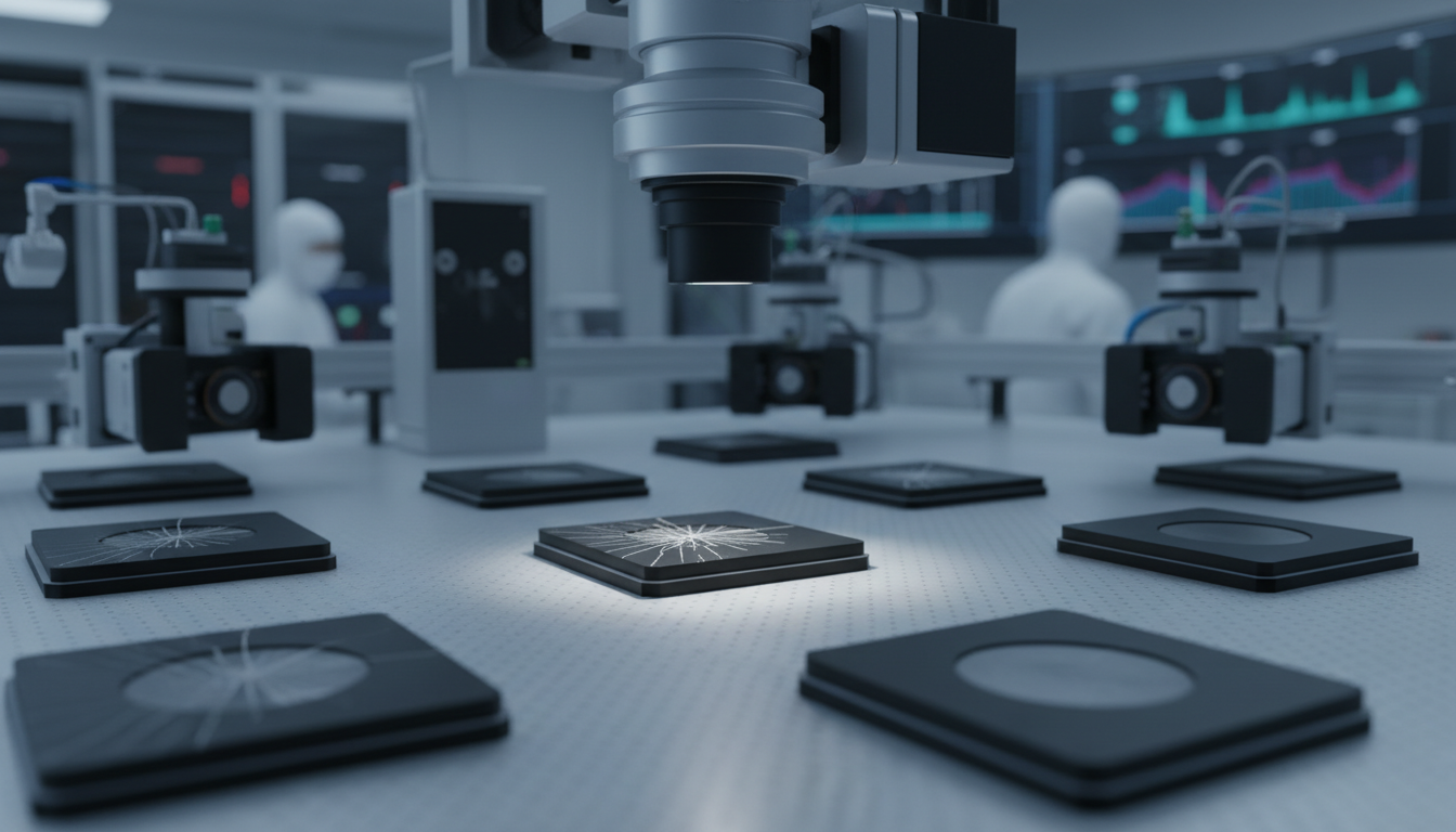
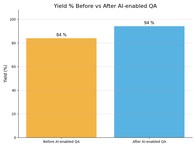
Integrating deep neural networks into our inspection flow has improved our defect detection rate by over 30% compared to prior techniques, enabling more reliable identification of cracks and irregularities on silicon wafers.
– C.C. Wei, CEO of TSMCCompliance Case Studies

Elevate your Silicon Wafer Engineering with AI-driven crack detection solutions. Stay ahead of the competition and ensure unparalleled quality in your production process.
Take Test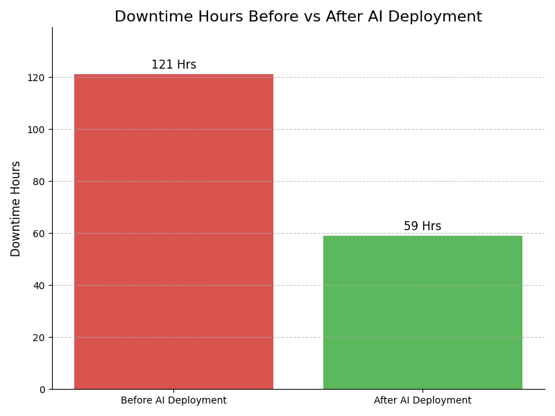
Leadership Challenges & Opportunities
Data Processing Bottlenecks
Implement AI Vision Crack Detection to automate and expedite the analysis of silicon wafer images. Utilize real-time data processing and machine learning algorithms to quickly identify cracks, thus significantly reducing processing time and enhancing throughput in wafer production.
Change Management Resistance
Facilitate AI Vision Crack Detection adoption by fostering a culture of innovation through workshops and training sessions. Engage employees early in the process to gather feedback and address concerns, ensuring the transition is perceived as an opportunity for growth rather than a disruption.
High Initial Investment
Utilize AI Vision Crack Detection in a phased approach, starting with critical areas that deliver immediate value. Explore leasing options or partnerships to distribute costs over time, allowing for budget-friendly integration while demonstrating ROI through improved defect detection.
Regulatory Compliance Challenges
Integrate AI Vision Crack Detection with compliance management systems to ensure adherence to industry standards. Automate documentation and reporting processes, leveraging AI's analytical capabilities to provide insights that help maintain compliance while minimizing manual effort.
Assess how well your AI initiatives align with your business goals
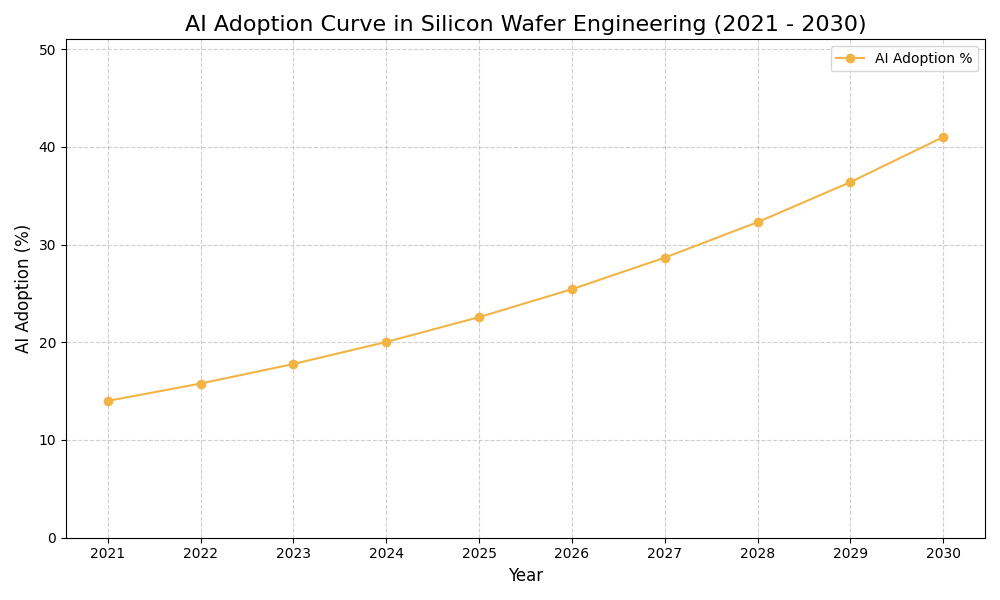
AI Adoption Graph
AI Use Case vs ROI Timeline
| AI Use Case | Description | Typical ROI Timeline | Expected ROI Impact |
|---|---|---|---|
| Automated Crack Detection | AI systems analyze images of silicon wafers to detect cracks automatically, reducing human error. For example, an AI tool can examine thousands of wafers per hour, identifying defects quickly and ensuring quality control during production. | 6-12 months | High |
| Predictive Maintenance Alerts | Using historical data and AI, companies can predict when equipment is likely to fail due to crack formation. For example, predictive models can alert operators to schedule maintenance before a wafer production machine breaks down. | 12-18 months | Medium-High |
| Enhanced Quality Assurance | AI algorithms can assess wafer quality by detecting micro-cracks that are invisible to the naked eye. For example, an AI system can provide real-time feedback to operators, ensuring only high-quality wafers proceed to the next stage. | 6-12 months | High |
| Streamlined Inspection Processes | Integrating AI in inspection processes reduces the time taken for quality checks. For example, AI-enabled vision systems can complete inspections in minutes instead of hours, increasing throughput in wafer production. | 3-6 months | Medium-High |
Glossary
Work with Atomic Loops to architect your AI implementation roadmap — from PoC to enterprise scale.
Contact NowFrequently Asked Questions
- AI Vision Crack Detection utilizes advanced algorithms for identifying defects in silicon wafers.
- This technology enhances product quality, ensuring high standards in wafer manufacturing.
- It minimizes human error, increasing reliability in quality assurance processes.
- Real-time monitoring allows for immediate corrective actions, improving operational efficiency.
- The integration of AI leads to reduced waste and optimized resource utilization.
- Start by assessing your current quality control systems and identifying gaps in performance.
- Engage with AI specialists to evaluate suitable technologies for your specific needs.
- Pilot projects can help test the effectiveness of AI solutions on a smaller scale.
- Training staff on new systems is crucial for smooth integration and operation.
- Gradually scale up the implementation based on feedback and performance metrics.
- AI enhances precision in defect detection, leading to higher product yield rates.
- Companies can achieve significant cost savings through reduced manual inspection efforts.
- The technology enables faster production cycles, increasing overall throughput.
- Data insights from AI systems facilitate informed strategic decisions and improvements.
- Organizations gain a competitive edge by consistently delivering high-quality products.
- Resistance to change from staff can hinder the successful implementation of AI technologies.
- Data quality and availability are critical; poor data can lead to inaccurate results.
- Integration with existing systems may require additional resources and time.
- Training and upskilling employees are necessary to maximize AI benefits.
- Regular evaluations and adjustments are crucial to address any emerging challenges.
- Investing is ideal when current processes show inefficiencies or high defect rates.
- A review of your quality control performance can indicate readiness for AI adoption.
- Market competitiveness often necessitates timely upgrades to advanced technologies.
- Align investments with organizational goals for quality improvement and innovation.
- Consider industry trends that emphasize automation and AI integration as strategic priorities.
- Compliance with ISO and industry-specific standards is essential for maintaining quality.
- Benchmarking against leading companies can offer insights into best practices and technologies.
- Regular audits and updates to systems ensure alignment with evolving standards.
- Collaboration with industry partners can aid in meeting regulatory requirements.
- Adopting standardized AI solutions can facilitate smoother integration and scalability.