
AI Throughput Wafer Max
AI Throughput Wafer Max represents a pivotal innovation in Silicon Wafer Engineering, integrating artificial intelligence to enhance wafer processing capabilities. This concept embodies the use of advanced algorithms and machine learning techniques to optimize throughput, ensuring that production aligns with the increasing demands of modern semiconductor applications. By focusing on AI implementation, stakeholders can better navigate the complexities of manufacturing processes, making this approach essential as the sector embraces digital transformation and seeks operational excellence.
In the evolving landscape of Silicon Wafer Engineering, AI Throughput Wafer Max is instrumental in redefining competitive strategies and fostering innovation. The integration of AI not only accelerates production efficiency but also enhances decision-making processes, enabling companies to respond swiftly to market changes. As organizations adopt these AI-driven practices, they encounter both promising growth opportunities and challenges, such as the intricacies of technology integration and shifting stakeholder expectations. This balance of optimism and realism underscores the transformative potential of AI in shaping the future of wafer engineering .
Harness AI for Unmatched Throughput in Silicon Wafer Engineering
Companies in the Silicon Wafer Engineering industry should engage in strategic investments and partnerships focused on AI-driven initiatives to optimize throughput in wafer manufacturing . By implementing advanced AI technologies, businesses can enhance production efficiency, reduce costs, and gain a significant competitive edge in the market.
How is AI Transforming Silicon Wafer Engineering?
Implementation Framework
Evaluate current infrastructure and skills
Develop a comprehensive data framework
Integrate AI algorithms in processes
Track AI-driven outcomes continuously
Enhance logistics and resource allocation
Conduct a comprehensive assessment of existing capabilities and infrastructure to identify gaps in AI readiness , ensuring alignment with AI Throughput Wafer Max objectives to enhance operational efficiency and competitiveness.
Industry Standards
Establish a robust data collection and management strategy to ensure high-quality, relevant data is available for AI algorithms, driving improvements in throughput and wafer quality across production processes.
Technology Partners
Implement AI algorithms across key operational processes, enabling real-time optimization and predictive analytics that enhance throughput and reduce defects in silicon wafer manufacturing and processing operations.
Internal R&D
Establish a continuous monitoring system to measure the performance of AI implementations, allowing for timely adjustments to enhance effectiveness and ensure alignment with overall supply chain goals and AI objectives.
Cloud Platform
Utilize AI insights to optimize supply chain logistics and resource allocation, improving responsiveness and efficiency while reducing lead times in silicon wafer engineering , thus achieving higher throughput and cost-effectiveness.
Industry Standards
Best Practices for Automotive Manufacturers
Integrate AI Algorithms Effectively
- Impact : Enhances defect detection accuracy significantly
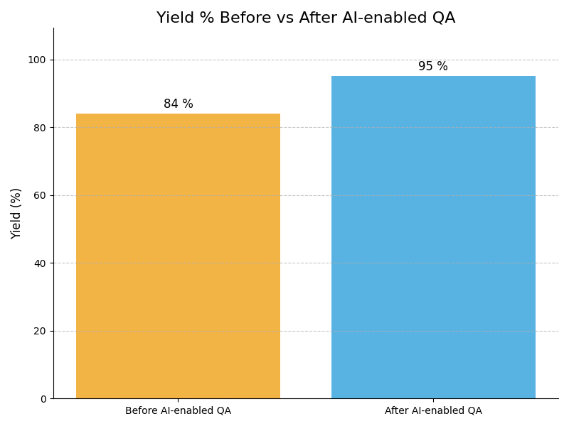
Example : Example: In a silicon wafer fabrication plant, an AI algorithm detects microscopic defects on wafers during the inspection process, improving accuracy by 30% compared to manual inspections, resulting in higher yield rates. - Impact : Reduces production downtime and costs
Example : Example: An AI system implemented in a manufacturing line predicts maintenance needs, reducing unplanned downtime by 25% and saving the company thousands in lost production each month. - Impact : Improves quality control standards
Example : Example: By utilizing AI for real-time quality checks, a semiconductor manufacturer reduces the need for manual inspections, improving quality control standards by ensuring every wafer is thoroughly checked before shipping. - Impact : Boosts overall operational efficiency
Example : Example: An AI-driven optimization system increases throughput by dynamically adjusting production schedules based on real-time demand, significantly boosting overall operational efficiency.
- Impact : High initial investment for implementation
Example : Example: A leading silicon wafer manufacturer postpones AI adoption after calculating costs for new AI software and hardware, exceeding budget allocations and delaying potential productivity gains. - Impact : Potential data privacy concerns
Example : Example: During AI trials, a manufacturer discovers that the system collects sensitive production data, leading to potential data privacy issues that require immediate attention and policy updates. - Impact : Integration challenges with existing systems
Example : Example: An AI solution fails to integrate with aging manufacturing execution systems, causing delays in data flow and necessitating costly upgrades to existing technology. - Impact : Dependence on continuous data quality
Example : Example: A manufacturing facility finds that fluctuations in environmental conditions lead to inconsistent data quality, causing AI misclassifications and impacting production quality.
Utilize Predictive Maintenance Tools
- Impact : Minimizes unexpected equipment failures
Example : Example: A silicon wafer plant employs predictive maintenance tools that analyze machine data to foresee failures. The result is a 40% reduction in unexpected breakdowns, leading to smoother operations and increased productivity. - Impact : Extends lifespan of production machinery
Example : Example: By using AI-driven analytics, a manufacturer extends the lifespan of their etching machines by 20%, allowing for longer production runs without significant capital expenditure on replacements. - Impact : Improves scheduling of maintenance tasks
Example : Example: An AI system predicts when specific machinery needs maintenance, improving scheduling accuracy by 30%. This ensures that maintenance is performed during non-peak hours, reducing overall downtime. - Impact : Reduces overall operational costs
Example : Example: A semiconductor manufacturing facility uses predictive analytics to optimize maintenance schedules, resulting in a 15% reduction in operational costs and better resource allocation.
- Impact : Cost of system updates and training
Example : Example: A semiconductor company faces challenges with the high costs associated with upgrading their predictive maintenance systems, which leads to delays in implementation and missed productivity opportunities. - Impact : Reliance on technology for decision-making
Example : Example: Over-reliance on predictive maintenance technology leads a wafer fabrication plant to overlook manual inspections, resulting in undetected issues that cause production delays. - Impact : Potential for inaccurate predictive data
Example : Example: An AI maintenance system fails to accurately predict a machinery breakdown due to insufficient data, resulting in an unexpected shutdown that halts production. - Impact : Risk of underestimating maintenance needs
Example : Example: A manufacturer underestimates the maintenance needs of older machines, leading to unexpected failures that disrupt operations and affect production timelines.
Implement Automated Quality Checks
- Impact : Increases inspection speed and accuracy
Example : Example: A silicon wafer manufacturer utilizes automated quality checks to inspect every wafer at high speeds, increasing inspection accuracy by 35% and significantly improving throughput during peak production. - Impact : Reduces human error in manufacturing
Example : Example: An AI-driven quality control system reduces human error in inspections, resulting in a 50% decline in defects and ensuring that only compliant wafers reach the market. - Impact : Enhances compliance with industry standards
Example : Example: By automating quality checks, a semiconductor company enhances compliance with rigorous industry standards, ensuring that all products meet necessary regulations before reaching customers. - Impact : Boosts customer satisfaction levels
Example : Example: A manufacturer reports a boost in customer satisfaction after implementing automated quality checks, as consistent product quality leads to fewer complaints and higher loyalty among clients.
- Impact : Dependence on AI systems for quality
Example : Example: A wafer fabrication facility experiences reliance on AI for quality, causing panic when the system encounters glitches, leading to production delays and increased scrutiny from management. - Impact : Potential integration issues
Example : Example: Integration issues arise when attempting to connect new automated quality systems with legacy equipment, resulting in unexpected delays and additional costs for the manufacturer. - Impact : High costs of automation technology
Example : Example: The high costs associated with implementing automation technology lead to budget overruns for a semiconductor company, forcing them to reconsider their investment strategy. - Impact : Disruption during implementation phase
Example : Example: A company faces temporary disruptions during the rollout of automated quality checks, as staff adapts to new procedures, impacting production schedules and output for several weeks.
Train Workforce Regularly
- Impact : Enhances team adaptability to AI tools
Example : Example: A silicon wafer plant invests in regular training sessions for its workforce, leading to a 30% increase in adaptability to new AI tools , resulting in optimized production processes. - Impact : Improves overall production efficiency
Example : Example: By improving workforce skills through training, a semiconductor manufacturer sees a 20% improvement in overall production efficiency, significantly elevating their output capacity and reducing waste. - Impact : Fosters a culture of continuous learning
Example : Example: Regular training fosters a culture of continuous learning, encouraging employees to embrace technological advancements, which increases innovation and collaboration across teams. - Impact : Reduces resistance to technological change
Example : Example: A training program reduces employee resistance to new AI technologies, resulting in a smoother transition during implementation and minimizing operational disruptions.
- Impact : Training costs can be substantial
Example : Example: A silicon wafer manufacturer realizes that training costs spiral out of control, impacting the budget for other critical projects and delaying overall operational improvements. - Impact : Time away from production during training
Example : Example: Production lines slow down as employees attend training programs, leading to temporary drops in output and increased pressure on remaining staff to meet production quotas. - Impact : Employee turnover may hinder effectiveness
Example : Example: High employee turnover rates at a semiconductor company impede the effectiveness of training programs, with new hires requiring additional training and reducing overall productivity. - Impact : Potential for inconsistent training quality
Example : Example: A training program implemented inconsistently across shifts leads to varying levels of proficiency among employees, causing confusion and inefficiencies on the production floor.
Optimize Data Management Systems
- Impact : Improves data accuracy and reliability
Example : Example: A silicon wafer manufacturer optimizes its data management system, resulting in a 25% increase in data accuracy. This improvement leads to more reliable reporting and better decision-making across departments. - Impact : Facilitates better decision-making processes
Example : Example: By enhancing data management processes, a semiconductor company facilitates quicker and more informed decision-making, leading to a 15% reduction in production errors and faster response times. - Impact : Enhances traceability of production data
Example : Example: Improved traceability in production data allows a manufacturer to quickly identify and rectify issues affecting quality, contributing to a 30% increase in customer satisfaction ratings. - Impact : Reduces data storage costs
Example : Example: Optimizing data management systems helps a company cut data storage costs by 20%, freeing up resources for investment in other critical technology upgrades.
- Impact : Complexity of data integration
Example : Example: A semiconductor manufacturer struggles with the complexity of integrating multiple data sources, leading to delays in project timelines and increased frustration among data analysts. - Impact : Data breaches pose significant risks
Example : Example: A data breach at a silicon wafer company exposes sensitive production information, causing reputational damage and leading to increased scrutiny from regulatory bodies. - Impact : High costs associated with upgrades
Example : Example: The high costs associated with upgrading data management systems strain the budget of a semiconductor company, forcing them to delay other important initiatives while they prioritize data integration. - Impact : Dependence on skilled personnel
Example : Example: Dependence on skilled personnel for managing data systems becomes a bottleneck when key employees leave the company, leading to gaps in knowledge and operational inefficiencies.
Leverage Real-time Analytics Tools
- Impact : Enables proactive problem-solving
Example : Example: A silicon wafer production facility implements real-time analytics tools that allow operations managers to identify and resolve production bottlenecks immediately, increasing overall efficiency. - Impact : Enhances operational visibility
Example : Example: With enhanced operational visibility through real-time data, a semiconductor manufacturer successfully responds to market changes, adjusting production schedules to meet varying demands and increasing profits. - Impact : Increases responsiveness to market changes
Example : Example: By leveraging real-time analytics, a company can quickly adapt its strategies to market trends, resulting in an improved competitive edge and increased market share. - Impact : Supports strategic planning efforts
Example : Example: Real-time analytics support strategic planning, allowing managers to make data-driven decisions that align production goals with market needs, improving overall business performance.
- Impact : Overwhelming amount of data generated
Example : Example: A semiconductor manufacturing plant faces challenges managing the overwhelming amount of data generated by real-time analytics, leading to confusion and delays in decision-making processes. - Impact : Potential for misinterpretation of data
Example : Example: Misinterpretation of analytics data at a silicon wafer company results in poor operational decisions, causing production slowdowns and increasing operational costs in the long run. - Impact : Costs associated with analytics tools
Example : Example: The costs associated with implementing advanced analytics tools strain the budget of a semiconductor company, necessitating cuts to other essential projects. - Impact : Dependence on technology for insights
Example : Example: Over-dependence on technology for insights leads to lapses in human judgment, as operators may overlook critical qualitative aspects that data alone cannot capture.
We manufactured the most advanced AI chips in the world, in the most advanced fab in the world, here in America for the first time, marking the beginning of an AI industrial revolution with unprecedented wafer production throughput.
– Jensen Huang, CEO of NVIDIACompliance Case Studies


Harness AI Throughput Wafer Max to revolutionize your silicon wafer engineering . Gain a competitive edge and achieve remarkable efficiency today—don’t be left behind!
Take Test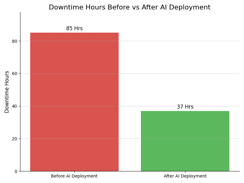
Leadership Challenges & Opportunities
Data Integration Challenges
Utilize AI Throughput Wafer Max to create a unified data ecosystem, enabling seamless integration of disparate data sources. Implement real-time analytics and predictive modeling to enhance decision-making. This approach minimizes data silos and enhances operational efficiency across Silicon Wafer Engineering processes.
Change Management Resistance
Foster a culture of innovation by implementing AI Throughput Wafer Max with user-friendly interfaces and comprehensive training. Engage stakeholders through regular updates and feedback sessions to address concerns. This strategy encourages acceptance of AI technologies, aligning workforce capabilities with evolving operational needs.
High Implementation Costs
Adopt AI Throughput Wafer Max using modular deployment strategies to spread costs over time. Focus on deploying high-impact features first, which yield immediate benefits, thus justifying further investment. This phased approach lowers initial financial barriers and demonstrates ROI quickly, facilitating broader adoption.
Talent Shortage in AI
Leverage AI Throughput Wafer Max to automate routine tasks, allowing existing staff to focus on higher-value activities. Invest in partnerships with educational institutions for talent development and internships. This strategy builds a skilled workforce while maximizing the benefits of AI-driven efficiencies in Silicon Wafer Engineering.
Assess how well your AI initiatives align with your business goals
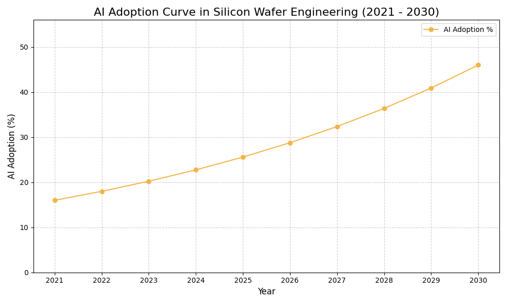
AI Adoption Graph
AI Use Case vs ROI Timeline
| AI Use Case | Description | Typical ROI Timeline | Expected ROI Impact |
|---|---|---|---|
| Predictive Maintenance for Equipment | AI algorithms analyze equipment data to predict failures before they occur. For example, using machine learning to monitor wafer fabrication machines helps in scheduling maintenance, reducing downtime and operational costs. | 6-12 months | High |
| Yield Optimization through Data Analytics | Leveraging AI to analyze production data enhances yield rates. For example, AI can identify patterns in defect data from wafer production, leading to adjustments in processes that optimize yield. | 12-18 months | Medium-High |
| Automated Quality Inspection | AI-driven visual inspection systems identify defects in wafers with high accuracy. For example, using computer vision to automate the inspection process reduces human error and speeds up quality control. | 6-12 months | Medium |
| Supply Chain Optimization | AI models predict demand and improve supply chain efficiency. For example, real-time data analysis helps in managing inventory levels of raw materials used in wafer production, reducing costs and waste. | 12-18 months | Medium-High |
Glossary
Work with Atomic Loops to architect your AI implementation roadmap — from PoC to enterprise scale.
Contact NowFrequently Asked Questions
- AI Throughput Wafer Max enhances wafer production efficiency through intelligent automation.
- It utilizes machine learning algorithms to optimize throughput and reduce cycle times.
- The technology improves yield rates by identifying potential defects early in the process.
- Organizations benefit from lower operational costs and increased production capacity.
- Overall, it fosters innovation and competitiveness in the semiconductor industry.
- Begin with a comprehensive assessment of current operational workflows and data systems.
- Engage stakeholders to identify specific areas where AI can add value.
- Pilot projects can help in testing AI solutions without full-scale implementation.
- Ensure that staff receives adequate training to adapt to new technologies.
- Iterate based on feedback and continuously refine AI applications for optimal results.
- Companies report increased production efficiency and reduced lead times significantly.
- Enhanced decision-making capabilities lead to improved yield and quality control.
- AI-driven insights facilitate faster innovation and responsiveness to market changes.
- Cost reductions in labor and material waste contribute to better profit margins.
- Ultimately, businesses gain a competitive edge in a rapidly evolving industry.
- Common obstacles include resistance to change from staff and unclear objectives.
- Data quality issues can hinder effective AI model training and deployment.
- Integration with legacy systems may require significant time and resources.
- Compliance with industry regulations must be carefully navigated to avoid pitfalls.
- Developing a clear strategy helps mitigate risks and enhances success rates.
- Organizations should consider adoption when experiencing production bottlenecks or inefficiencies.
- A readiness assessment can help determine technological and operational maturity.
- Emerging market demands often signal the need for rapid innovation capabilities.
- Timing can also depend on available budget and resources for implementation.
- Staying ahead of competitors is crucial, making timely adoption beneficial.
- Compliance with data protection regulations is essential when integrating AI technologies.
- Organizations must adhere to industry standards for quality and safety benchmarks.
- Regular audits and assessments help ensure ongoing compliance with regulations.
- Transparency in AI decision-making processes builds trust with stakeholders.
- Engaging with legal experts early in the process can prevent future complications.
- Monitor key performance indicators like yield rates and cycle times for insights.
- Benchmark against industry standards to evaluate the effectiveness of AI implementations.
- Regularly assess operational costs to ensure AI technology delivers expected ROI.
- Engage with industry peers to share best practices and insights on AI usage.
- Continuous improvement initiatives can help maintain competitive performance levels.