
AI Process Control Silicon Guide
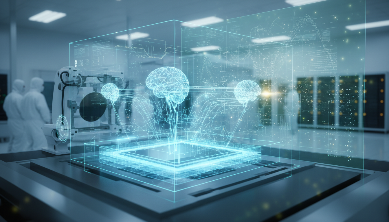
In the realm of Silicon Wafer Engineering, the " AI Process Control Silicon Guide" represents a pivotal framework that integrates artificial intelligence into manufacturing processes. This guide delineates the methodologies and technologies that enable enhanced precision and efficiency in wafer production . As the sector evolves, the relevance of this guide becomes increasingly apparent to stakeholders who are navigating the intersection of traditional engineering practices and cutting-edge AI innovations . Embracing this guide is crucial for aligning with the broader trends of AI-led transformation, which are reshaping operational efficiencies and strategic priorities in the field.
The Silicon Wafer Engineering ecosystem is undergoing a significant shift driven by AI-enabled practices that redefine how stakeholders interact and innovate. The implementation of AI is not merely a technical upgrade; it is a fundamental change that enhances decision-making, operational efficiency, and overall product quality. As organizations adopt these AI-driven approaches, they unlock new avenues for growth while simultaneously facing challenges such as integration complexities and evolving expectations. The path forward is filled with opportunities, but it requires a nuanced understanding of the balance between optimistic advancements and the realistic hurdles that come with them.
Accelerate AI Adoption in Silicon Wafer Engineering
Companies in the Silicon Wafer Engineering industry should strategically invest in AI-driven process control technologies and forge partnerships with leading AI firms to enhance production efficiency. Implementing these AI strategies is expected to yield significant improvements in operational performance, cost reduction, and a stronger competitive edge in the market.
How AI is Transforming Silicon Wafer Engineering?
Implementation Framework
Evaluate current AI capabilities and infrastructure
Create a comprehensive AI implementation plan
Deploy AI technologies across operations
Enhance workforce skills for AI adoption
Continuously evaluate AI performance
Conduct a thorough assessment of existing AI capabilities and infrastructure in silicon wafer engineering to identify gaps and opportunities. This ensures alignment with AI-driven goals and enhances operational efficiency, guiding future investments.
Technology Partners
Formulate a detailed AI strategy incorporating best practices tailored for silicon wafer engineering . This strategy should prioritize key areas for AI integration, ensuring smoother transitions and maximizing technological benefits for competitive advantage.
Industry Standards
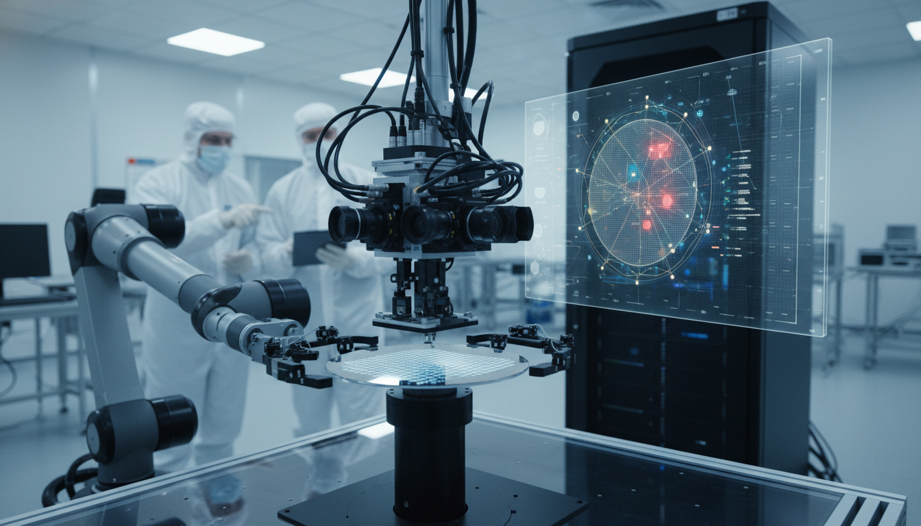
Integrate AI solutions into silicon wafer manufacturing processes, focusing on predictive analytics and automation. This increases production efficiency and product quality while addressing challenges like supply chain disruptions through enhanced decision-making capabilities.
Internal R&D
Provide comprehensive training programs for staff on AI technologies and their applications in silicon wafer engineering . This empowers employees, facilitates smooth transitions, and encourages innovation within the organization, ensuring long-term success.
Cloud Platform
Establish a system for ongoing monitoring and optimization of AI implementations in silicon wafer processes. Regular assessments ensure alignment with business goals, identifying areas for improvement and maintaining competitive advantages in a dynamic market.
Industry Standards
Best Practices for Automotive Manufacturers
Integrate AI Algorithms Effectively
- Impact : Enhances defect detection accuracy significantly
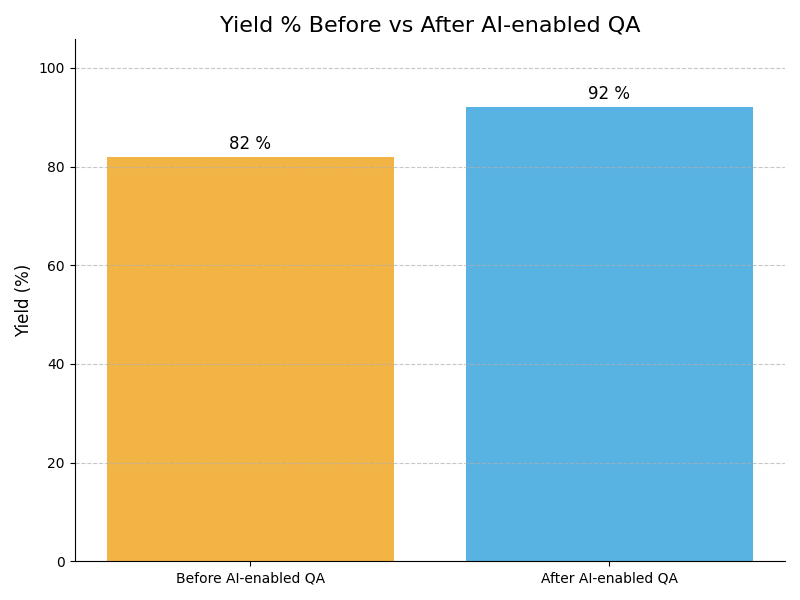
Example : Example: In a semiconductor fabrication facility, AI algorithms analyze wafer images in real-time, detecting microscopic defects that human inspectors overlook, leading to a 30% reduction in defective wafers produced. - Impact : Reduces production downtime and costs
Example : Example: A silicon wafer manufacturer employs AI to optimize machine settings automatically. This adjustment minimizes downtime by 20%, allowing for a smoother production flow and increased output. - Impact : Improves quality control standards
Example : Example: By implementing AI-driven quality control, a wafer processing plant reduces the rate of product recalls, improving customer satisfaction and trust in their brand. - Impact : Boosts overall operational efficiency
Example : Example: Machine learning models dynamically adjust inspection parameters based on real-time production data, resulting in a significant increase in throughput without sacrificing quality.
- Impact : High initial investment for implementation
Example : Example: A leading semiconductor company faced delays in AI implementation after realizing that the costs for advanced sensors and software exceeded initial budget forecasts, pushing back their timeline significantly. - Impact : Potential data privacy concerns
Example : Example: An AI-driven quality control system inadvertently collects sensitive operational data, raising alarms about data privacy compliance and prompting a review of the company’s data handling practices. - Impact : Integration challenges with existing systems
Example : Example: A silicon wafer manufacturer struggled with integrating new AI tools with existing legacy systems, leading to production delays and requiring additional resources to bridge the technological gap. - Impact : Dependence on continuous data quality
Example : Example: An AI system in a fabrication plant fails due to poor data quality from outdated sensors, causing misclassification of acceptable products as defective, resulting in unnecessary production halts.
Utilize Real-time Monitoring
- Impact : Enables proactive issue detection and resolution
Example : Example: A silicon wafer plant implements real-time monitoring, allowing technicians to detect temperature fluctuations instantly, preventing potential equipment failures before they escalate into costly downtime. - Impact : Improves operational visibility across teams
Example : Example: Production teams at a semiconductor facility use real-time dashboards to track yield rates, enabling quick adjustments and improving overall throughput by 15% within the first quarter. - Impact : Facilitates timely decision-making processes
Example : Example: An AI system provides real-time insights into production lines, allowing managers to make informed decisions on resource allocation, thereby reducing waste and optimizing output. - Impact : Enhances equipment maintenance scheduling
Example : Example: By employing real-time monitoring tools, a wafer manufacturing facility has enhanced its predictive maintenance capabilities, reducing unplanned machine downtime by 25%.
- Impact : Requires robust infrastructure for data collection
Example : Example: A semiconductor manufacturer invests heavily in data collection infrastructure but experiences network issues, resulting in incomplete data streams that hinder effective monitoring. - Impact : Possible over-reliance on automated systems
Example : Example: An operations team becomes overly reliant on automated alerts from real-time systems, leading to a decrease in human oversight and critical thinking during production. - Impact : Data overload from excessive monitoring
Example : Example: A wafer fabrication facility faces data overload from numerous monitoring systems, making it difficult for operators to identify actionable insights amidst the noise. - Impact : Challenges in user training and adaptation
Example : Example: Employees at a silicon wafer plant struggle to adapt to new monitoring technologies, leading to initial resistance and reduced efficiency during the transition period.
Train Workforce Regularly
- Impact : Ensures effective AI tool utilization
Example : Example: A silicon wafer factory implements ongoing training sessions, ensuring employees can effectively use AI systems, resulting in a 20% decrease in operational errors within six months. - Impact : Boosts employee morale and engagement
Example : Example: Regular training workshops on AI tools enhance employee confidence and engagement, fostering a collaborative environment that drives innovation and productivity. - Impact : Promotes a culture of continuous improvement
Example : Example: A company promotes continuous improvement culture through monthly training, empowering employees to identify and suggest process enhancements, leading to a 10% efficiency increase. - Impact : Reduces operational errors and inefficiencies
Example : Example: After implementing a comprehensive training program, a semiconductor plant sees a significant drop in errors, directly correlating to improved quality control and customer satisfaction.
- Impact : Training programs can be time-consuming
Example : Example: A silicon wafer manufacturer faces delays in AI implementation due to extensive training requirements, causing production timelines to stretch beyond initial estimates. - Impact : Resistance to change among staff
Example : Example: Employees at a semiconductor facility resist adopting AI tools, creating friction within teams and slowing down innovation efforts as they cling to familiar methods. - Impact : High costs associated with comprehensive training
Example : Example: A company incurs high costs for specialized training programs, straining budgets without immediate visible returns on investment in operational improvements. - Impact : Potential skill gaps if not updated regularly
Example : Example: An engineering team struggles with new AI tools because training sessions become outdated, leading to skill gaps that hinder productivity and innovation efforts.
Implement Feedback Loops
- Impact : Enhances AI system learning and adaptation
Example : Example: A silicon wafer company incorporates feedback loops into its AI systems, allowing for rapid learning from production data, leading to a 30% increase in yield rates over six months. - Impact : Facilitates continuous process optimization
Example : Example: By establishing regular feedback sessions between operators and data scientists, a semiconductor plant optimizes processes continually, reducing waste by 15% annually. - Impact : Improves collaboration between teams
Example : Example: A collaboration platform enables cross-team feedback on AI performance, fostering innovation and driving enhancements that significantly improve operational efficiency. - Impact : Drives innovation through iterative improvements
Example : Example: An AI-driven process control system evolves through user feedback, leading to timely updates that enhance defect detection and overall product quality.
- Impact : Requires time and resources for effective implementation
Example : Example: A semiconductor manufacturer struggles to allocate time for feedback processes, leading to stagnation in AI system improvements and operational inefficiencies. - Impact : Difficulties in gathering actionable feedback
Example : Example: Gathering actionable feedback proves challenging as operators are often too busy with day-to-day tasks, leading to missed opportunities for system enhancement. - Impact : Potential for conflicting feedback from teams
Example : Example: Conflicting feedback from different teams creates confusion regarding the direction of AI system updates, slowing down progress and causing frustration. - Impact : Slower decision-making during feedback evaluation
Example : Example: A silicon wafer plant experiences slower decision-making due to prolonged evaluations of feedback, resulting in missed opportunities for timely improvements.
Leverage Predictive Analytics
- Impact : Improves forecasting accuracy for production
Example : Example: A silicon wafer manufacturer employs predictive analytics to optimize production schedules, resulting in a 25% improvement in forecasting accuracy and reduced excess inventory. - Impact : Reduces waste through proactive decision-making
Example : Example: By using predictive maintenance analytics, a semiconductor facility identifies equipment failures before they occur, decreasing unplanned downtime by 30% in one year. - Impact : Helps identify potential equipment failures
Example : Example: A wafer processing plant utilizes predictive analytics to streamline resource allocation, leading to a significant reduction in material waste and increased operational efficiency. - Impact : Enables better resource allocation strategies
Example : Example: Predictive analytics allows a silicon wafer manufacturer to forecast demand trends accurately, enabling timely adjustments that optimize production and minimize costs.
- Impact : Requires high-quality historical data
Example : Example: A semiconductor manufacturer faces challenges in developing predictive models due to incomplete historical data, resulting in unreliable forecasts and poor production planning. - Impact : Complexity in model development and validation
Example : Example: The complexity of predictive analytics models leads to difficulties in validation, causing delays in implementation and uncertainty in decision-making. - Impact : Potential misinterpretation of predictive results
Example : Example: A silicon wafer plant misinterprets predictive results, leading to overproduction of certain products and increased costs due to unsold inventory. - Impact : Dependence on accurate data inputs
Example : Example: The accuracy of predictive analytics is compromised by poor data input quality, resulting in misguided operational strategies and wasted resources.
We manufactured the most advanced AI chips in the world, in the most advanced fab in the world, here in America for the first time, marking the beginning of AI-driven semiconductor process advancements.
– Jensen Huang, CEO of NvidiaCompliance Case Studies


Harness the power of AI to elevate your Silicon Wafer Engineering . Transform operations, gain a competitive edge , and start achieving remarkable results today.
Take Test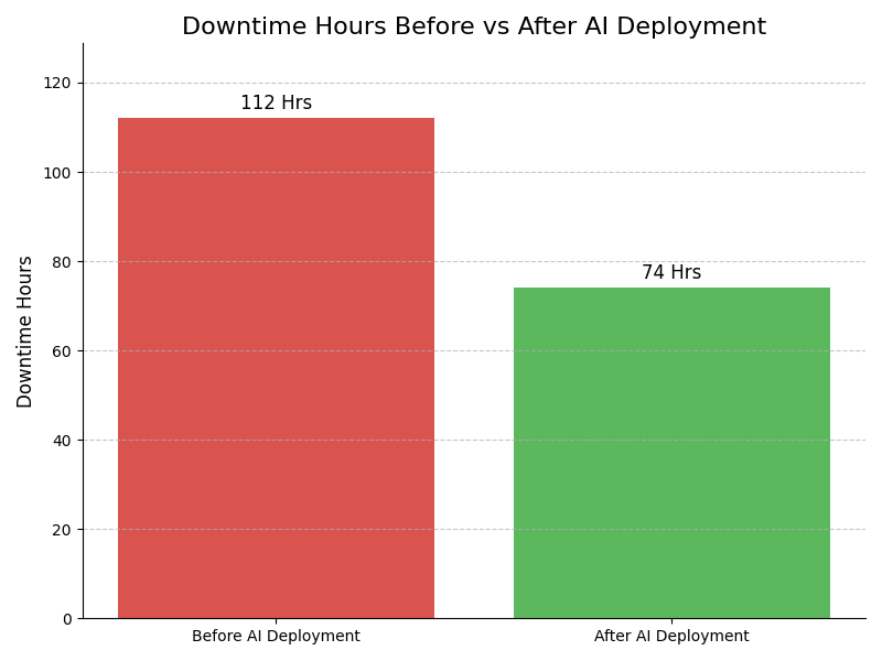
Leadership Challenges & Opportunities
Data Integrity Challenges
Utilize AI Process Control Silicon Guide's advanced data validation algorithms to ensure high-quality data inputs during silicon wafer manufacturing. Implement real-time analytics to monitor data flows and automatically flag discrepancies, enhancing decision-making and reducing errors in production.
Cultural Resistance to Change
Facilitate the adoption of AI Process Control Silicon Guide by introducing change management initiatives that emphasize the technology's benefits. Engage stakeholders through workshops and pilot projects that showcase tangible improvements, fostering a culture of innovation and collaboration within the Silicon Wafer Engineering teams.
High Implementation Costs
Leverage AI Process Control Silicon Guide's modular architecture to implement solutions incrementally, reducing upfront costs. Focus on prioritizing high-impact areas first, and utilize cloud-based services to minimize infrastructure investment while maximizing scalability and ROI in Silicon Wafer Engineering operations.
Regulatory Compliance Burdens
Employ AI Process Control Silicon Guide's compliance tracking features to automate documentation and reporting processes in Silicon Wafer Engineering. This technology helps maintain adherence to industry regulations by providing real-time insights and alerts for compliance-related issues, streamlining operational workflows.
Assess how well your AI initiatives align with your business goals
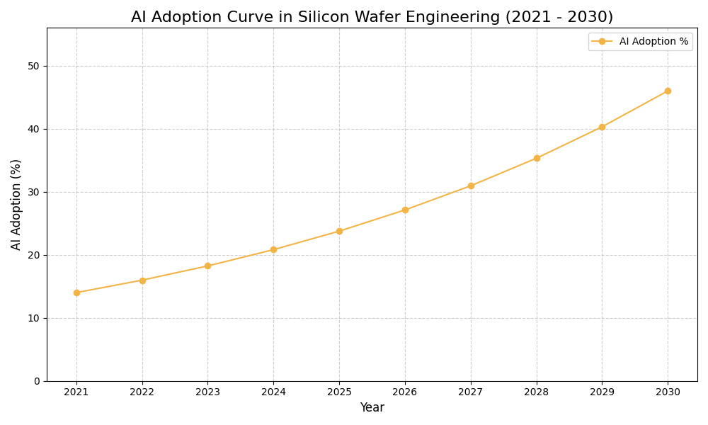
AI Adoption Graph
AI Use Case vs ROI Timeline
| AI Use Case | Description | Typical ROI Timeline | Expected ROI Impact |
|---|---|---|---|
| Predictive Maintenance for Equipment | AI algorithms analyze sensor data to predict equipment failures before they occur, minimizing downtime. For example, using predictive analytics on wafer fabrication machinery helps schedule maintenance proactively, ensuring continuous production flow. | 6-12 months | High |
| Yield Optimization through Machine Learning | Machine learning models optimize production parameters to enhance yield rates in silicon wafer fabrication. For example, adjusting temperature and pressure based on real-time data can significantly reduce defects and improve output quality. | 12-18 months | Medium-High |
| Defect Detection using Computer Vision | AI-driven computer vision systems automatically inspect silicon wafers for defects during production. For example, deploying image recognition software to identify impurities can drastically reduce the need for manual inspections and improve quality assurance. | 6-12 months | High |
| Supply Chain Forecasting with AI | AI analyzes historical data and market trends to forecast demand and optimize inventory levels. For example, using AI to predict silicon wafer demand can streamline procurement processes and reduce excess inventory costs. | 12-18 months | Medium-High |
Glossary
Work with Atomic Loops to architect your AI implementation roadmap — from PoC to enterprise scale.
Contact NowFrequently Asked Questions
- AI Process Control Silicon Guide integrates AI to enhance manufacturing efficiency and precision.
- It optimizes process parameters through real-time data analysis and machine learning algorithms.
- Companies can achieve higher yields and lower defect rates in silicon wafer production.
- The guide facilitates better resource management, reducing operational costs significantly.
- Ultimately, it supports innovation by enabling faster adaptation to market changes.
- Begin by assessing your current systems and identifying potential integration points.
- Engage stakeholders early to ensure alignment and gather necessary resources.
- Develop a phased implementation plan focusing on pilot projects to test concepts.
- Consider partnerships with AI technology providers for expertise and support.
- Continuous training and change management are crucial for successful adoption across teams.
- Organizations can expect improved yield rates, measured through defect density reductions.
- Operational costs typically decrease due to streamlined processes and resource optimization.
- Enhanced data analytics capabilities lead to more informed decision-making and forecasting.
- Customer satisfaction often improves due to higher quality and faster delivery times.
- Regular performance reviews ensure alignment with strategic goals and continuous improvement.
- Common obstacles include resistance to change from staff and existing cultural norms.
- Integration with legacy systems can pose technical challenges and require careful planning.
- Data quality issues may arise, necessitating thorough cleansing and validation processes.
- Ensuring compliance with industry regulations is essential and can complicate implementation.
- Establishing clear metrics for success helps in navigating these challenges effectively.
- Investing in AI enhances competitive advantage by streamlining operations and reducing costs.
- The technology drives innovation, enabling faster cycles for product development and deployment.
- It improves quality assurance through predictive maintenance and real-time monitoring.
- AI capabilities empower teams to make data-driven decisions, enhancing responsiveness.
- Ultimately, a well-implemented approach leads to sustainable growth and market leadership.
- The ideal time to adopt AI is when existing processes show inefficiencies or high defect rates.
- Organizations should consider readiness, including technological infrastructure and team capabilities.
- Market pressures and competition often signal the need for timely technological upgrades.
- Pilot projects can help gauge organizational readiness and potential benefits.
- Regular assessments of operational performance can guide the timing for adoption.
- Benchmarking against industry leaders can provide insights into best practices and performance metrics.
- Key areas to measure include yield rates, defect densities, and operational costs.
- Adopting best practices from successful implementations can shorten learning curves.
- Regulatory compliance benchmarks ensure adherence to industry standards during implementation.
- Continuous evaluation against these benchmarks drives ongoing improvements and innovation.