
AI Plasma Etch Optimization
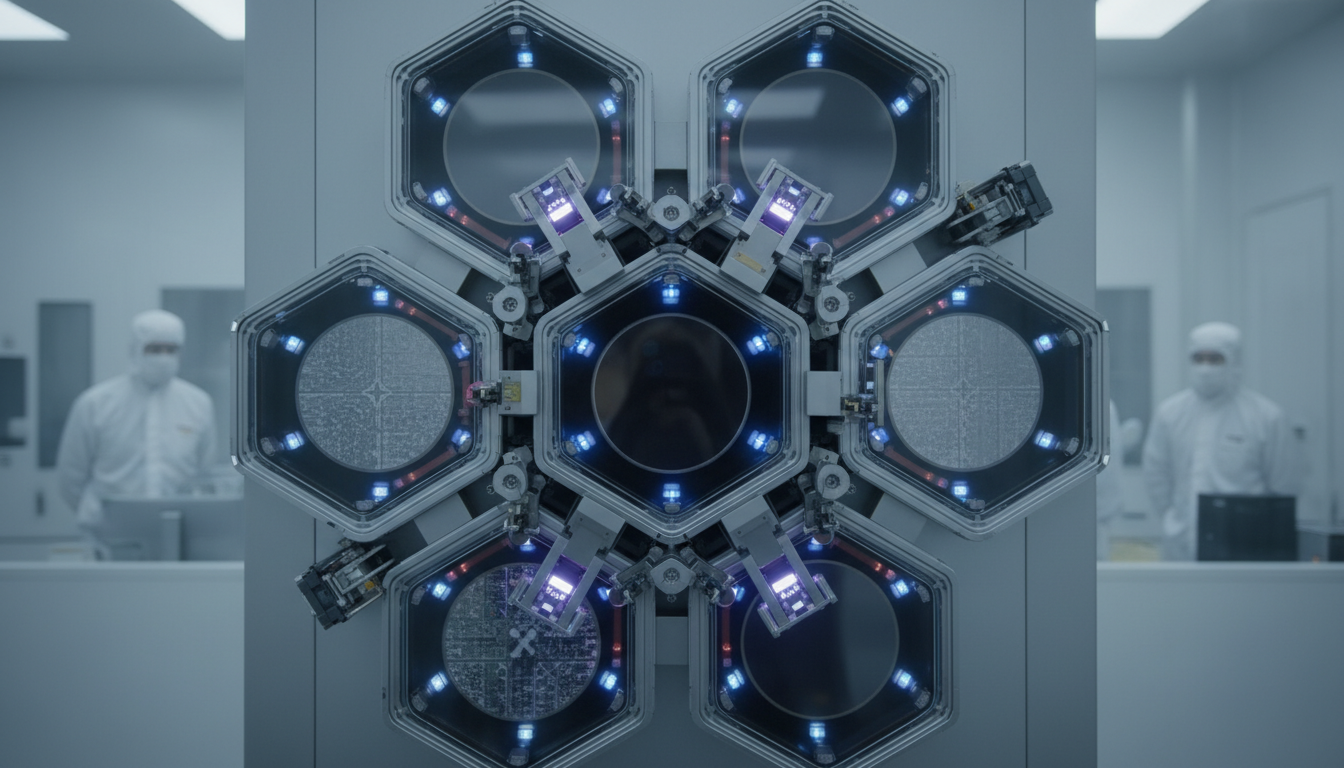
AI Plasma Etch Optimization is a transformative practice within the Silicon Wafer Engineering sector, focusing on enhancing the precision and efficiency of the etching process through artificial intelligence technologies. This approach not only refines the manufacturing of semiconductor wafers but also aligns with the broader trend of AI integration across various technological domains. As industries strive for greater operational excellence, the relevance of AI Plasma Etch Optimization becomes increasingly pronounced, offering stakeholders innovative pathways to enhance production quality and reduce lead times.
The Silicon Wafer Engineering ecosystem is undergoing significant changes driven by AI Plasma Etch Optimization, reshaping how organizations compete and innovate. AI-driven methodologies enhance decision-making processes and operational efficiency, fostering a more agile and responsive environment. As stakeholders embrace these advancements, they are presented with both opportunities for growth and challenges, such as the complexities of integration and evolving expectations. This dynamic interplay signifies a pivotal moment in the sector, where strategic adaptation to AI technologies can lead to sustained competitive advantages.
Maximize Efficiency through AI Plasma Etch Optimization
Silicon Wafer Engineering companies should strategically invest in AI-driven Plasma Etch Optimization technologies and form partnerships with leading AI firms to enhance their manufacturing processes. Implementing AI can significantly boost process efficiency, reduce costs, and provide a competitive advantage in the fast-evolving semiconductor market.
How AI is Transforming Plasma Etch Optimization in Silicon Wafer Engineering
Implementation Framework
Combine data analytics with AI algorithms
Establish continuous data collection systems
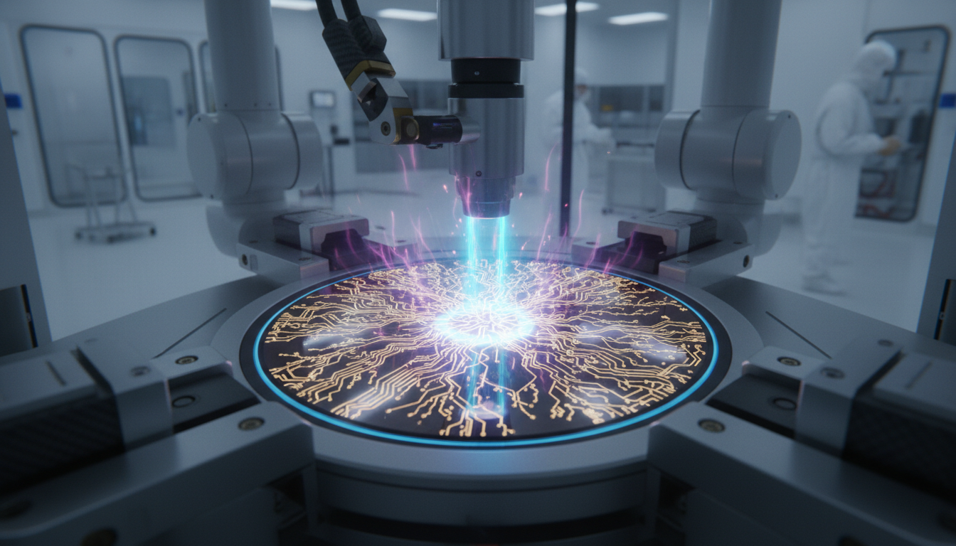
Use AI to refine etching conditions
Leverage AI for equipment upkeep
Streamline collaboration through AI tools
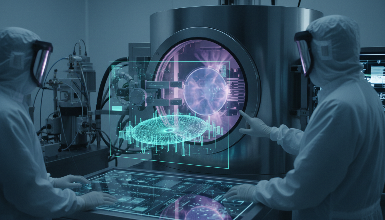
Integrating AI models into plasma etch processes enhances decision-making through data-driven insights, optimizing parameters like pressure and gas flow, ensuring consistent wafer quality and increasing manufacturing efficiency while addressing variability challenges.
Technology Partners
Establishing real-time monitoring systems enables continuous data collection during plasma etch processes, facilitating immediate adjustments and enhancing operational efficiency while addressing issues promptly, thereby minimizing waste and downtime.
Industry Standards
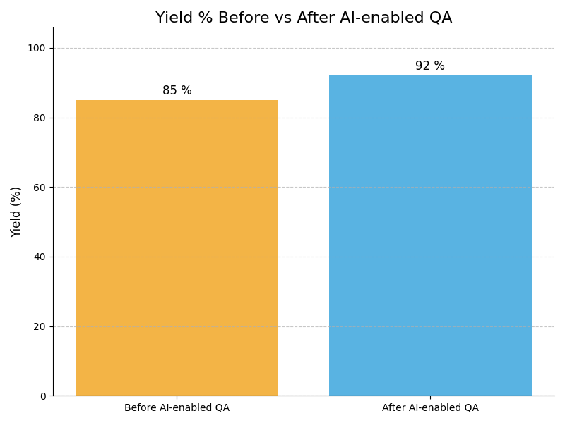
Utilizing AI to optimize etching parameters like temperature, pressure, and gas composition can significantly reduce defects and increase yield, enhancing overall productivity and ensuring high-quality silicon wafers while mitigating operational risks.
Internal R&D
Implementing predictive maintenance strategies using AI algorithms helps anticipate equipment failures before they occur, reducing downtime and maintenance costs, thus ensuring smooth operations and enhancing the reliability of plasma etch processes.
Cloud Platform
Integrating AI tools within the supply chain fosters collaboration between suppliers and manufacturers, streamlining communication and improving responsiveness to market demands, thus enhancing overall agility and competitiveness in Silicon Wafer Engineering .
Technology Partners
Best Practices for Automotive Manufacturers
Utilize AI-Driven Analytics
- Impact : Improves process efficiency and speed
Example : Example: A silicon wafer fabrication plant implemented AI analytics to monitor etch rates, leading to a 20% increase in production speed while reducing chemical waste by 15%. - Impact : Reduces material waste and costs
Example : Example: An electronics manufacturer used AI-driven analytics to identify underperforming equipment, allowing for predictive maintenance that cut down equipment failures by 30%. - Impact : Enables predictive maintenance scheduling
Example : Example: AI analytics helped to optimize the etching process, allowing a semiconductor company to reduce material waste by 25%, saving substantial costs on raw materials. - Impact : Enhances decision-making with data insights
Example : Example: A wafer fabrication facility integrated AI insights into their decision-making process, which led to a 40% reduction in production downtimes due to informed operational adjustments. - Impact : Streamlines workflow and operational processes
Example : Example: By streamlining workflows with AI, a semiconductor company managed to enhance their operational processes, leading to a 15% increase in yield rates and outperforming competitors. - Impact : Facilitates real-time performance monitoring
Example : Example: A silicon wafer engineering firm adopted real-time performance monitoring through AI, resulting in rapid issue identification and a subsequent 20% reduction in process delays. - Impact : Boosts yield rates through optimization
Example : Example: An AI system optimized etching parameters, resulting in a 10% yield improvement and establishing the company as a leader in high-quality wafer products. - Impact : Enhances competitive edge in market
Example : Example: AI-driven process streamlining allowed a wafer manufacturer to reduce cycle times significantly, gaining a competitive edge in meeting customer demands faster.
- Impact : Requires continuous algorithm retraining
Example : Example: A semiconductor manufacturer faced challenges when their AI model became outdated, requiring extensive retraining that delayed production schedules and increased costs. - Impact : Potential for over-reliance on technology
Example : Example: Over-reliance on AI led a wafer company to overlook human insights, resulting in an undetected defect that compromised product quality and customer trust. - Impact : High costs for data acquisition
Example : Example: Costs for acquiring high-quality data for AI training proved to be higher than anticipated, forcing a silicon manufacturer to revise their project budget significantly. - Impact : Integration complexities with legacy systems
Example : Example: A legacy system's inability to integrate with new AI tools created a bottleneck in data flow, which hindered timely decision-making and operational efficiency.
Implement Real-time Monitoring Solutions
- Impact : Enhances defect detection capabilities
Example : Example: A silicon wafer manufacturer installed real-time monitoring sensors that detected defects instantly, increasing defect detection rates by 30% compared to previous methods. - Impact : Improves operational transparency
Example : Example: Implementing real-time monitoring provided a semiconductor company with transparency in their processes, allowing for immediate corrections and improving overall operational efficiency by 25%. - Impact : Reduces response time to issues
Example : Example: Real-time issue monitoring cut down response times significantly, allowing an electronics manufacturer to address production problems within minutes, enhancing customer satisfaction with timely deliveries. - Impact : Increases customer satisfaction and trust
Example : Example: A wafer fabrication facility experienced an increase in customer satisfaction as real-time data monitoring led to consistent product quality, strengthening client relationships. - Impact : Facilitates proactive issue resolution
Example : Example: Proactive issue resolution through real-time monitoring allowed a semiconductor plant to identify potential equipment failures before they occurred, saving costs on emergency repairs. - Impact : Supports compliance with industry standards
Example : Example: A silicon wafer company used real-time data to ensure compliance with industry standards, which led to a successful audit and maintained their market reputation. - Impact : Optimizes resource allocation
Example : Example: Real-time monitoring enabled optimal resource allocation in a fabrication plant, resulting in a 15% reduction in operational costs while maximizing output. - Impact : Enhances collaboration among teams
Example : Example: Enhanced team collaboration occurred as real-time data sharing improved communication between departments, leading to more synchronized efforts in production optimization.
- Impact : Data overload can hinder analysis
Example : Example: A silicon wafer facility faced data overload from real-time monitoring systems, making it difficult for teams to analyze critical information, leading to missed opportunities for optimization. - Impact : Potential for system failures
Example : Example: System failures in real-time monitoring equipment caused significant production downtimes for a semiconductor manufacturer, highlighting the vulnerability of relying on technology without backup plans. - Impact : High dependency on accurate sensors
Example : Example: Dependency on highly accurate sensors led to issues when faulty sensors provided misleading data, resulting in production errors and increased scrap rates. - Impact : Challenges in maintaining data integrity
Example : Example: A silicon wafer manufacturer struggled to maintain data integrity across multiple systems, which resulted in inconsistent reporting and challenges in effective decision-making.
Train Workforce on AI Tools
- Impact : Improves employee engagement and morale
Example : Example: A semiconductor firm trained its workforce on AI tools, leading to a 20% increase in employee engagement and satisfaction, as workers felt more competent in their roles. - Impact : Enhances workforce skill sets
Example : Example: Training initiatives improved workforce skills in a silicon wafer company, resulting in a 15% increase in efficiency as employees effectively utilized AI tools in their daily tasks. - Impact : Increases efficiency in AI usage
Example : Example: A wafer fabrication facility noticed a significant drop in operational errors after implementing comprehensive AI training programs for their employees, enhancing overall productivity. - Impact : Reduces operational errors significantly
Example : Example: Empowering employees through AI training created a culture of innovation in a semiconductor company, allowing teams to leverage new technologies effectively and boost performance. - Impact : Requires investment in training programs
Example : Example: A silicon wafer manufacturer faced challenges when investing heavily in training programs, as some employees resisted adapting to new AI technologies, slowing implementation. - Impact : Resistance to change from employees
Example : Example: Resistance to change became apparent in a semiconductor company, where employees were reluctant to embrace AI tools, causing delays in the optimization process. - Impact : Time-consuming training schedules
Example : Example: Time-consuming training schedules impacted production timelines for a wafer fabrication facility, creating a temporary dip in output during the transition to AI tools. - Impact : Potential for skill gaps in workforce
Example : Example: A skills gap emerged in a silicon wafer company when older workers struggled to adapt to new AI systems, prompting concerns about overall operational efficiency.
- Impact : Training costs can escalate quickly
Example : Example: A semiconductor manufacturer faced escalating training costs as they expanded their AI education programs, impacting overall project budgets and resource allocation. - Impact : Potential misalignment with business goals
Example : Example: Misalignment with business goals occurred when a silicon wafer company invested in AI training unrelated to their operational needs, wasting valuable time and resources. - Impact : Difficulty in assessing training effectiveness
Example : Example: Assessing training effectiveness proved difficult for a wafer fabrication facility, as they struggled to measure improvements in productivity or error rates post-training. - Impact : Dependence on key personnel for knowledge
Example : Example: A heavy dependence on key personnel in a semiconductor company for AI knowledge transfer led to vulnerabilities, as knowledge gaps emerged when those individuals left the organization.
Establish Cross-functional Collaboration
- Impact : Enhances innovation through diverse perspectives
Example : Example: Cross-functional teams in a silicon wafer company collaborated on AI projects, leading to innovative solutions that improved etching processes by 30% through diverse input. - Impact : Improves problem-solving capabilities
Example : Example: Problem-solving capabilities improved in a semiconductor firm as cross-functional collaboration allowed teams to address issues more effectively, reducing downtime by 15%. - Impact : Fosters a culture of continuous improvement
Example : Example: A culture of continuous improvement flourished when departments in a wafer fabrication facility shared insights, resulting in a 20% increase in operational efficiency over a year. - Impact : Aligns goals across departments
Example : Example: Aligning goals across departments in a semiconductor company fostered a unified approach to AI implementation, streamlining processes and enhancing productivity. - Impact : Coordination challenges among teams
Example : Example: Coordination challenges arose in a silicon wafer company as teams struggled to align their efforts on AI projects, causing delays in implementation timelines. - Impact : Potential for conflicting priorities
Example : Example: Conflicting priorities emerged within a semiconductor firm, resulting in a lack of focus on critical AI initiatives and hindering overall progress. - Impact : Time-consuming decision-making processes
Example : Example: Time-consuming decision-making processes in a wafer fabrication facility slowed down the AI project timeline, as teams had difficulties reaching consensus on strategies. - Impact : Requires clear communication strategies
Example : Example: A lack of clear communication strategies led to misunderstandings in a semiconductor company, resulting in misaligned objectives and wasted resources on AI initiatives.
- Impact : Requires ongoing commitment from leadership
Example : Example: Ongoing commitment from leadership was essential for a silicon wafer company, as a leadership change led to a shift in focus, jeopardizing cross-functional projects. - Impact : Potential for miscommunication across teams
Example : Example: Miscommunication across teams in a semiconductor company created confusion regarding AI project goals, resulting in wasted time and resources on initiatives that were not aligned. - Impact : Difficulty in managing team dynamics
Example : Example: Managing team dynamics proved challenging in a wafer fabrication facility, as differing viewpoints occasionally led to conflicts that hindered collaboration effectiveness. - Impact : High reliance on collaborative tools
Example : Example: High reliance on collaborative tools in a semiconductor firm created challenges when technical issues arose, disrupting the communication flow and delaying project timelines.
Integrate AI into Quality Control
- Impact : Boosts defect detection rates significantly
Example : Example: AI integration into quality control at a silicon wafer facility boosted defect detection rates by 40%, significantly reducing the need for manual inspections. - Impact : Reduces costs associated with rework
Example : Example: A semiconductor manufacturer reduced costs associated with rework by 30% after implementing AI-driven quality control systems that minimized errors during production. - Impact : Enhances overall product quality
Example : Example: Enhanced overall product quality was achieved when a wafer fabrication company utilized AI for real-time quality assessments, leading to fewer customer complaints and returns. - Impact : Enables faster time-to-market
Example : Example: Faster time-to-market was realized in a semiconductor firm as AI-driven quality control streamlined processes, allowing products to reach customers ahead of competitors. - Impact : Requires careful calibration of AI systems
Example : Example: A silicon wafer company faced challenges in calibrating their AI systems accurately, leading to initial inconsistencies in quality assessments and production delays. - Impact : Initial resistance from quality control teams
Example : Example: Initial resistance from quality control teams slowed down AI implementation in a semiconductor manufacturer, as employees were hesitant to trust automated systems over traditional methods. - Impact : High costs associated with system upgrades
Example : Example: High costs associated with system upgrades became an issue for a wafer fabrication facility, straining budgets and delaying the rollout of AI quality initiatives. - Impact : Potential for over-dependence on technology
Example : Example: Over-dependence on AI technology in quality control led to a situation where manual checks were neglected, resulting in occasional lapses in product quality that raised concerns.
- Impact : Data bias can skew results
Example : Example: Data bias in the AI system of a silicon wafer manufacturer led to skewed results, resulting in missed defects that impacted the final product quality significantly. - Impact : Integration with existing quality systems
Example : Example: Integration challenges arose when attempting to merge AI systems with existing quality control processes in a semiconductor firm, delaying implementation and causing frustration. - Impact : Requires ongoing updates and maintenance
Example : Example: Ongoing updates and maintenance were required for an AI quality control system in a wafer fabrication facility, which proved to be time-consuming and resource-intensive. - Impact : Potential for false positives in detection
Example : Example: A high rate of false positives in defect detection arose in a semiconductor company, causing unnecessary rejections and slowing down the production line as teams adjusted thresholds.
AI is revolutionizing semiconductor manufacturing, including plasma etch processes, by enabling the production of the most advanced AI chips on US wafers for the first time, marking the start of a new industrial revolution.
– Jensen Huang, CEO of NVIDIACompliance Case Studies
Seize the opportunity to enhance your silicon wafer engineering with AI-driven plasma etch optimization. Transform your operations and stay ahead of your competition today.
Take Test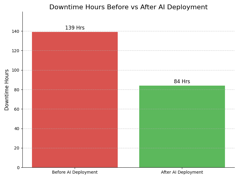
Leadership Challenges & Opportunities
Equipment Calibration Issues
Utilize AI Plasma Etch Optimization to automate and refine calibration processes for etching equipment. By integrating real-time data analytics and machine learning algorithms, organizations can achieve optimal equipment performance, reduce downtime, and ensure consistent etching results, enhancing overall production efficiency.
Change Management Resistance
Foster a culture of innovation by implementing AI Plasma Etch Optimization alongside change management initiatives. Engage stakeholders through workshops and training sessions, demonstrating the technology’s benefits. This approach builds trust and encourages acceptance, facilitating smoother transitions in Silicon Wafer Engineering operations.
High Operational Costs
Implement AI Plasma Etch Optimization to analyze and streamline processes, identifying key areas for cost reduction. By optimizing resource allocation and reducing waste through predictive maintenance, companies can achieve significant savings, ultimately lowering the total cost of ownership in Silicon Wafer Engineering.
Data Integration Challenges
Leverage AI Plasma Etch Optimization for seamless integration of disparate data sources within Silicon Wafer Engineering. Employ advanced data management strategies to unify and analyze information in real time, enhancing decision-making processes and improving operational efficiency across departments.
Assess how well your AI initiatives align with your business goals
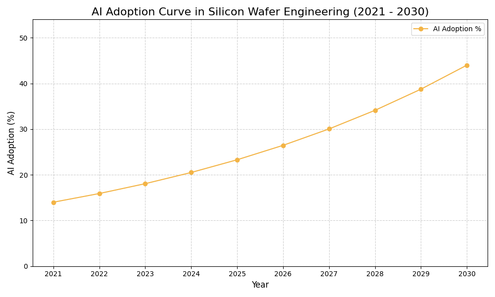
AI Adoption Graph
AI Use Case vs ROI Timeline
| AI Use Case | Description | Typical ROI Timeline | Expected ROI Impact |
|---|---|---|---|
| Process Parameter Optimization | AI algorithms analyze real-time data to optimize etching parameters, minimizing defects. For example, by adjusting gas flow rates based on feedback, manufacturers can achieve higher yield rates and reduce waste during production runs. | 6-12 months | High |
| Predictive Maintenance Scheduling | Utilizing AI to predict equipment failures before they occur helps reduce downtime. For example, predictive models can forecast when etching machines require maintenance, ensuring they operate efficiently without unexpected disruptions. | 12-18 months | Medium-High |
| Yield Prediction Analytics | AI models analyze historical data to predict wafer yield outcomes. For example, by assessing factors like temperature and pressure, companies can make informed decisions, improving overall product quality and profitability. | 6-12 months | Medium |
| Real-Time Quality Control | AI-driven systems monitor etching quality during production. For example, leveraging computer vision, systems can detect surface anomalies instantly, allowing for immediate corrective actions, thus enhancing product integrity. | 6-12 months | High |
Glossary
Work with Atomic Loops to architect your AI implementation roadmap — from PoC to enterprise scale.
Contact NowFrequently Asked Questions
- AI Plasma Etch Optimization uses algorithms to improve etching processes in silicon wafers.
- It minimizes defects and enhances precision through real-time monitoring and adjustments.
- Companies can achieve better yields and quality in semiconductor manufacturing.
- The technology also helps reduce material waste and operational costs effectively.
- Overall, it streamlines workflows, leading to faster production cycles and innovation.
- Begin by assessing your current processes and identifying areas needing improvement.
- Engage with AI technology providers for tailored solutions that fit your needs.
- Allocate resources and training for staff to ensure a smooth transition to AI integration.
- Establish clear goals and success metrics to measure the effectiveness of changes.
- Consider a pilot project to validate strategies before a full-scale rollout.
- You can anticipate improved wafer yield rates through enhanced process controls.
- Reduced cycle times lead to faster turnaround and increased production capacity.
- Operational costs often decrease due to minimized waste and resource usage.
- Data-driven insights help refine strategies and drive continuous improvements.
- Overall, businesses gain a competitive edge through enhanced product quality.
- Resistance to change from staff can hinder the adoption of new technologies.
- Integration issues with existing systems may complicate the implementation process.
- Data quality and availability are crucial for effective AI performance.
- Ensuring compliance with industry regulations and standards is essential.
- Continuous training and support are necessary to overcome initial hurdles.
- Investing in AI can lead to significant long-term cost savings and efficiency gains.
- It enhances the precision of processes, which is vital in semiconductor manufacturing.
- Companies can respond faster to market demands, improving their competitive stance.
- AI-driven insights facilitate better decision-making and strategic planning.
- Long-term benefits include sustainable growth and innovation capabilities.
- AI can optimize etching parameters for various materials used in semiconductor manufacturing.
- It is utilized in defect detection and classification during the etching process.
- Process optimization can enhance the performance of memory and logic devices.
- AI solutions can predict equipment failures, minimizing downtime and maintenance costs.
- Real-time data analytics support ongoing process improvements and innovation.
- Organizations should consider adoption when facing challenges in production efficiency.
- Timing is also influenced by advancements in AI technologies and market conditions.
- The readiness of existing systems to integrate AI is a critical factor.
- Evaluate the competitive landscape to determine urgency for innovation.
- A proactive approach can prevent falling behind industry standards and competitors.
- Establish a clear project roadmap with defined goals and timelines for implementation.
- Engage cross-functional teams to ensure diverse perspectives and expertise are included.
- Continuously monitor performance metrics to evaluate the effectiveness of AI solutions.
- Invest in staff training and development to foster a culture of innovation and adaptability.
- Regularly review and update strategies based on technological advancements and market needs.