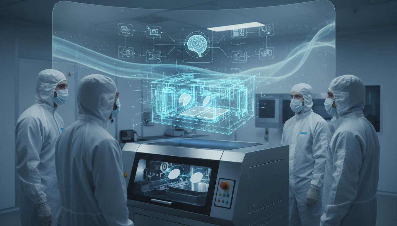
AI Multi Fab Wafer Sync
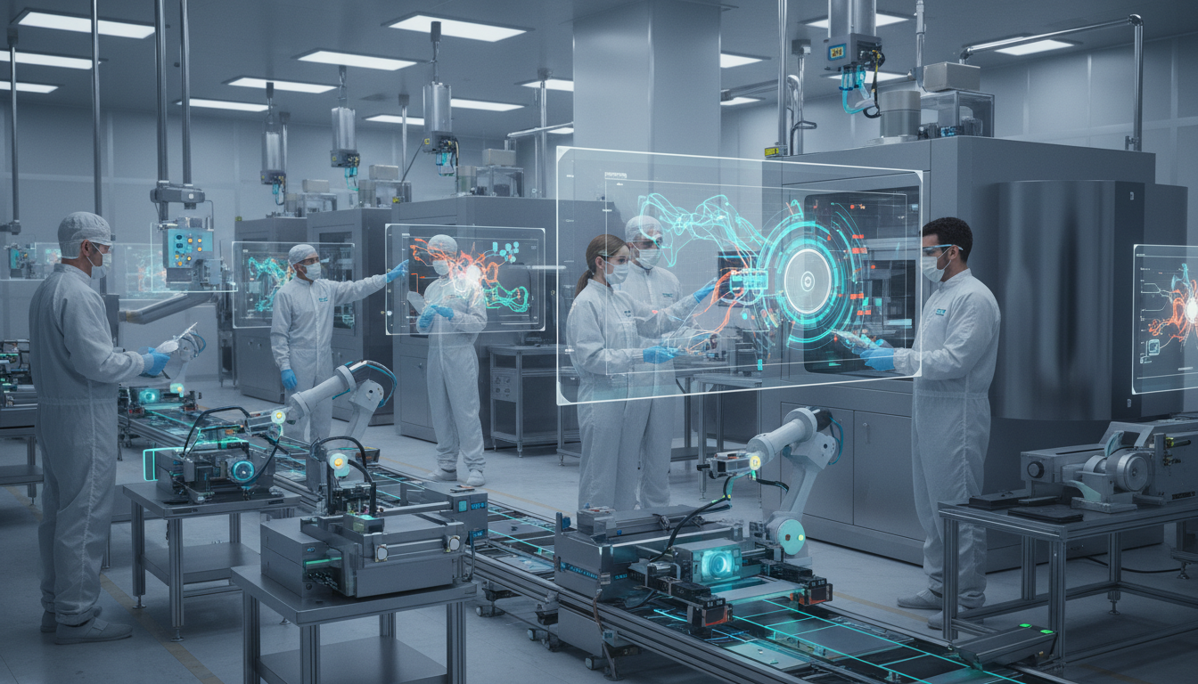
AI Multi Fab Wafer Sync represents a transformative approach in the Silicon Wafer Engineering landscape, harnessing artificial intelligence to synchronize operations across multiple fabrication facilities. This concept embodies the integration of advanced analytics and machine learning techniques to optimize wafer production processes, thereby enhancing operational efficiencies and quality control. As the semiconductor sector increasingly adopts AI , this synchronization becomes critical for stakeholders aiming to stay competitive in a rapidly evolving technological environment.
The significance of AI Multi Fab Wafer Sync extends beyond mere operational efficiency; it reshapes competitive dynamics and fosters collaborative innovation among stakeholders. By incorporating AI-driven methodologies, companies can improve decision-making processes, streamline communication, and enhance product development cycles. However, while the opportunities for growth are substantial, challenges such as integration complexities and shifting stakeholder expectations must be navigated carefully. This dual focus on potential and hurdles is essential for organizations looking to thrive in this AI-enhanced ecosystem.
Maximize Efficiency with AI Multi Fab Wafer Sync
Companies in the Silicon Wafer Engineering industry should strategically invest in AI-driven Multi Fab Wafer Sync technologies and forge partnerships with leading AI firms to enhance production capabilities. By implementing AI, businesses can expect significant gains in operational efficiency, cost reduction, and a strengthened competitive edge in the market.
How AI is Revolutionizing Silicon Wafer Engineering?
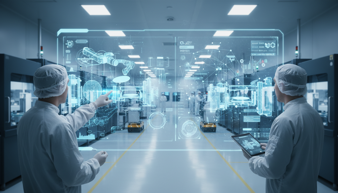
Implementation Framework
Combine AI with existing technologies
Leverage AI for enhanced insights
AI-driven maintenance strategies
AI for better stakeholder communication
AI for ongoing process improvement
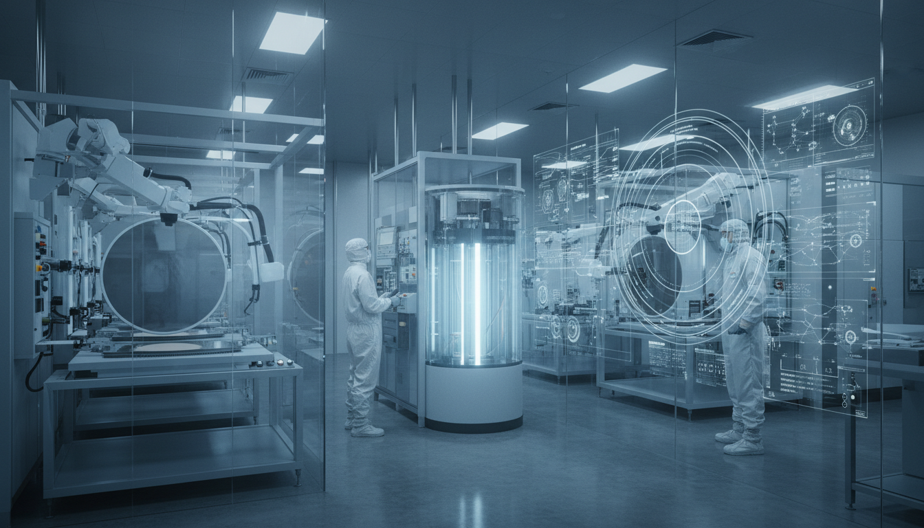
Integrating AI systems into existing Silicon Wafer Engineering processes enhances data processing capabilities, optimizing wafer production . This approach can significantly reduce downtime and improve operational efficiency, increasing overall yield and quality.
Industry Standards
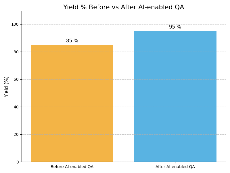
Utilizing AI-driven data analytics improves decision-making processes by providing actionable insights into production metrics, enabling engineers to identify inefficiencies and streamline operations, ultimately enhancing wafer quality and throughput .
Technology Partners
Implementing predictive maintenance powered by AI reduces unexpected equipment failures and maintenance costs. By analyzing real-time data, engineers can anticipate issues, ensuring continuous operations and improved reliability in wafer fabrication processes.
Internal R&D
Employing AI technologies for enhancing supply chain collaboration fosters better communication among stakeholders, leading to improved coordination and reduced lead times. This approach builds a more resilient supply chain for wafer production .
Industry Standards
Adopting continuous learning models utilizing AI allows for ongoing refinement in manufacturing processes by analyzing past performance data. This leads to systematic improvements, ensuring consistent wafer quality and operational efficiency over time.
Cloud Platform
Best Practices for Automotive Manufacturers
Implement Predictive Maintenance Strategies
- Impact : Reduces unplanned downtime significantly
Example : Example: A silicon wafer fabrication facility deployed AI-driven predictive maintenance, reducing unplanned downtime by 30% by anticipating equipment failures before they occur and scheduling timely maintenance. - Impact : Extends equipment lifespan and reliability
Example : Example: By analyzing sensor data, an AI system predicted a critical tool failure in a semiconductor plant, allowing for proactive maintenance that extended the tool's lifespan by an additional year. - Impact : Enhances overall system productivity
Example : Example: A wafer manufacturing site implemented AI to monitor equipment wear levels, resulting in a 25% increase in overall productivity as machines operated more efficiently without unexpected stops. - Impact : Lowers maintenance costs over time
Example : Example: By shifting to predictive maintenance, a fab reduced maintenance costs by 20%, as timely interventions prevented costly breakdowns and extended the life of key machinery.
- Impact : High initial investment for implementation
Example : Example: A silicon wafer producer faced a budget crisis when initial costs for AI integration, including software, sensors, and training, significantly exceeded projections, forcing a project delay. - Impact : Requires skilled personnel for operation
Example : Example: An advanced fab struggled to find qualified personnel to operate their new AI systems, leading to inefficiencies and increased reliance on external consultants, raising operational costs. - Impact : Data integration complexities in legacy systems
Example : Example: Integration of AI systems with a legacy wafer inspection tool failed due to compatibility issues, resulting in a costly overhaul of existing infrastructure to accommodate new technology. - Impact : Dependence on accurate data input quality
Example : Example: An AI system misinterpreted data from an outdated sensor, leading to incorrect maintenance alerts, which caused unnecessary downtime and wasted resources as teams scrambled to investigate.
Optimize AI-Driven Scheduling
- Impact : Enhances production line efficiency
Example : Example: A semiconductor foundry used AI to optimize scheduling, resulting in a 20% boost in production line efficiency as it adjusted workloads dynamically based on real-time data. - Impact : Improves resource allocation and utilization
Example : Example: By implementing AI-driven scheduling, a wafer fab improved resource allocation, reducing idle time by 15% and maximizing the use of available tools and personnel during peak production. - Impact : Reduces lead time for wafer processing
Example : Example: AI scheduling algorithms allowed a silicon wafer manufacturer to cut lead times by 10%, enabling faster response to urgent orders without compromising quality or throughput. - Impact : Increases responsiveness to market demand
Example : Example: An AI scheduling system adjusted to unexpected demand spikes, allowing a fab to redirect resources effectively and deliver products ahead of schedule, enhancing customer satisfaction.
- Impact : Potential resistance from workforce
Example : Example: A silicon wafer manufacturer faced pushback from employees resistant to adopting AI-driven scheduling, fearing job loss, which delayed implementation and affected morale. - Impact : Requires continuous model training
Example : Example: An AI scheduling model initially performed poorly due to insufficient training data, leading to production delays and requiring constant updates to improve accuracy and reliability. - Impact : Risk of over-automation in processes
Example : Example: A fab experienced workflow disruptions as over-automation in scheduling caused unforeseen bottlenecks, illustrating the need for human oversight in critical decision-making. - Impact : Misalignment with business goals
Example : Example: An AI scheduling initiative failed to align with the company’s strategic goals, resulting in a misallocation of resources that did not meet market demands or production targets.
Utilize Real-Time Data Analytics
- Impact : Improves decision-making speed
Example : Example: A silicon wafer production facility utilized real-time analytics, improving decision-making speed by 40%, allowing for immediate adjustments when quality anomalies were detected during processing. - Impact : Enhances process optimization capabilities
Example : Example: By leveraging real-time data analytics, a fab optimized its processes, achieving a 15% increase in yield as it identified and addressed inefficiencies promptly during production. - Impact : Increases yield through timely insights
Example : Example: An AI-driven analytics platform enabled a wafer manufacturer to implement proactive quality control, catching potential defects before reaching final inspection, reducing waste by 25%. - Impact : Facilitates proactive quality control
Example : Example: Real-time data insights allowed a fab to adjust parameters dynamically, improving overall process optimization and reducing cycle times by 20%, leading to increased throughput.
- Impact : High complexity in data management
Example : Example: A semiconductor plant struggled with managing vast amounts of real-time data, leading to complexity in analysis and delayed responses to production issues as analysts were overwhelmed. - Impact : Risk of data overload for analysts
Example : Example: An AI system provided too much data, resulting in analysis paralysis among engineers who struggled to identify actionable insights, delaying critical decisions and impacting productivity. - Impact : Dependence on stable internet connectivity
Example : Example: A wafer manufacturing facility faced significant disruptions when unstable internet connectivity interrupted access to real-time analytics, causing delays in responding to production anomalies. - Impact : Requires continuous monitoring and updates
Example : Example: Continuous monitoring and updates of the AI analytics system became resource-intensive, pulling staff away from other critical tasks and creating operational bottlenecks in the fab.
Integrate AI for Quality Assurance
- Impact : Enhances defect detection accuracy
Example : Example: A silicon wafer manufacturer integrated AI for quality assurance, achieving a 30% improvement in defect detection accuracy as AI algorithms identified issues that were previously overlooked by human inspectors. - Impact : Reduces human error in inspections
Example : Example: By using AI-driven quality assurance systems, a fab minimized human error during inspections, leading to a 25% reduction in rework and improving overall operational efficiency. - Impact : Improves compliance with industry standards
Example : Example: An AI quality assurance tool helped a semiconductor plant maintain compliance with stringent industry standards, ensuring consistent quality and reducing the risk of regulatory fines. - Impact : Boosts customer satisfaction with quality
Example : Example: Enhanced quality control through AI resulted in improved customer satisfaction levels, as clients reported fewer defects and higher product reliability, ultimately boosting sales by 15%.
- Impact : Potential bias in AI algorithms
Example : Example: A silicon wafer plant discovered that its AI quality assurance system was biased towards common defects, missing unique issues that traditional methods would have caught, leading to product recalls. - Impact : High dependency on historical data
Example : Example: An AI system relied heavily on historical data, resulting in inadequate detection of newly emerging defects, which caused unexpected quality issues and customer complaints. - Impact : Integration challenges with current QA systems
Example : Example: Integrating AI with existing quality assurance systems presented challenges, as legacy software incompatibility delayed the rollout and caused temporary disruptions in quality checks. - Impact : Risk of overlooking unique defects
Example : Example: The AI system’s focus on standard defects led to overlooking unique defects that required human judgment, resulting in a batch of wafers being shipped with undetected flaws.
Train Workforce Continuously
- Impact : Enhances employee adaptability to AI
Example : Example: A silicon wafer manufacturer implemented a continuous training program, enhancing employee adaptability to AI systems, resulting in a smoother transition and improved operational efficiency by 20%. - Impact : Improves overall team performance
Example : Example: Continuous training initiatives in a fab improved overall team performance as employees were better equipped to harness AI tools effectively, leading to innovative solutions and increased productivity. - Impact : Fosters innovation and collaboration
Example : Example: By fostering innovation through regular training sessions, a wafer manufacturing facility encouraged collaboration between teams, leading to the development of new techniques that enhanced production processes. - Impact : Reduces resistance to technological change
Example : Example: A proactive training approach reduced resistance to technological changes among employees, creating a culture of openness towards AI adoption and boosting morale across the workforce.
- Impact : Training costs can be significant
Example : Example: A semiconductor fab faced significant training costs when rolling out new AI systems, impacting budget allocations for other essential operational improvements and delaying progress. - Impact : Potential knowledge gaps in AI roles
Example : Example: Knowledge gaps emerged in key AI roles, as some employees were unable to keep pace with advancements, leading to reliance on external consultants for critical support and guidance. - Impact : Time-consuming implementation of training programs
Example : Example: The time-consuming implementation of training programs in a wafer production facility delayed the full deployment of AI initiatives, resulting in missed opportunities for immediate improvements. - Impact : Risk of outdated training materials
Example : Example: Outdated training materials in an AI course led to confusion among employees, causing inconsistencies in system usage and impacting overall productivity in the fab.
We manufactured the most advanced AI chips in the world, in the most advanced fab in the United States for the first time, marking the beginning of AI-driven wafer production here.
– Jensen Huang, CEO of NVIDIACompliance Case Studies
Embrace AI-driven solutions to enhance efficiency and precision in your processes. Don’t fall behind—seize the competitive edge in Silicon Wafer Engineering now!
Take Test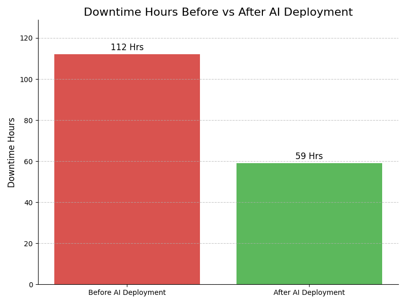
Leadership Challenges & Opportunities
Data Synchronization Delays
Implement AI Multi Fab Wafer Sync to streamline data synchronization across multiple fabs, reducing latency in real-time data processing. Utilize predictive analytics to forecast production needs and optimize scheduling, resulting in improved yield and reduced operational downtime throughout the wafer fabrication process.
Cultural Resistance to Change
Foster a cultural shift by integrating AI Multi Fab Wafer Sync in pilot projects to showcase quick wins. Engage employees through workshops and feedback sessions to demonstrate the technology’s benefits, easing concerns and encouraging adoption, ultimately leading to a more agile and innovative workforce.
High Initial Investment
Utilize AI Multi Fab Wafer Sync's flexible subscription model to mitigate high initial costs. Begin with targeted pilot projects that align with strategic goals and demonstrate ROI, enabling gradual scaling of investment while ensuring budget adherence and maximizing the financial impact of the technology.
Supply Chain Complexity
Employ AI Multi Fab Wafer Sync to enhance visibility and coordination across the supply chain. Leverage its predictive capabilities to optimize inventory management and streamline logistics, reducing delays and improving collaboration among suppliers, which in turn leads to better resource allocation and efficiency.
Assess how well your AI initiatives align with your business goals
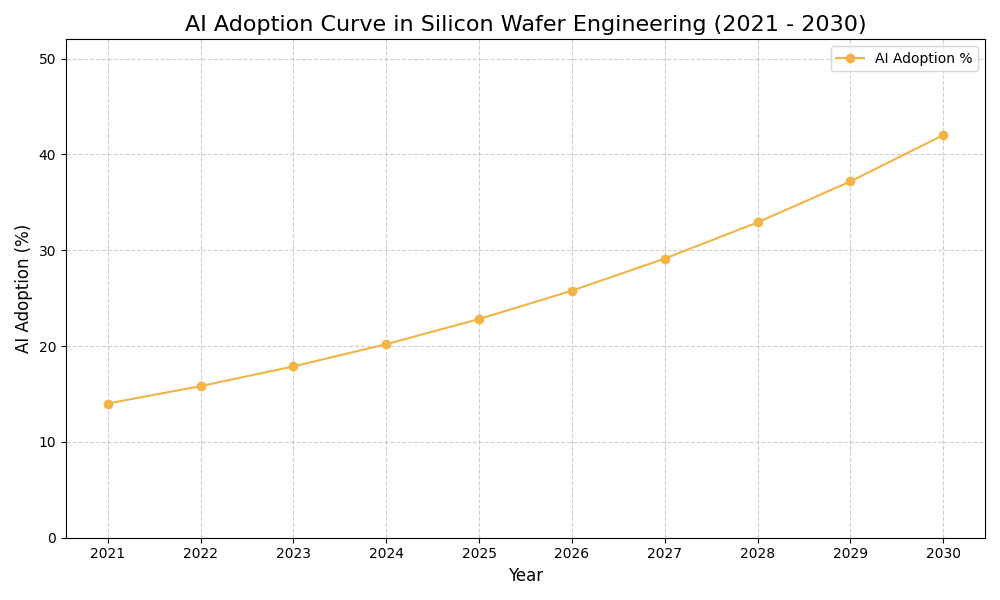
AI Adoption Graph
AI Use Case vs ROI Timeline
| AI Use Case | Description | Typical ROI Timeline | Expected ROI Impact |
|---|---|---|---|
| Automated Wafer Quality Inspection | AI algorithms analyze wafer images for defects in real-time, significantly reducing manual inspection time. For example, integrating AI-powered cameras can detect surface anomalies, ensuring only high-quality wafers proceed to production, enhancing yield rates. | 6-12 months | High |
| Predictive Maintenance for Fabrication Equipment | Using AI to predict equipment failures before they occur, thus minimizing downtime. For example, AI models analyze sensor data from fabrication machines to forecast maintenance schedules, ensuring continuous operation and reducing unexpected outages. | 12-18 months | Medium-High |
| Supply Chain Optimization for Wafer Production | AI optimizes supply chain logistics by predicting demand and adjusting inventory levels. For example, AI tools help semiconductor manufacturers align raw material deliveries with production schedules, significantly reducing holding costs and improving cash flow. | 6-12 months | Medium |
| Enhanced Process Control in Wafer Fabrication | AI systems monitor and adjust fabrication processes in real time to maintain optimal conditions. For example, AI algorithms can dynamically regulate temperature and pressure in etching processes, reducing variability and improving product consistency. | 12-18 months | High |
Glossary
Work with Atomic Loops to architect your AI implementation roadmap — from PoC to enterprise scale.
Contact NowFrequently Asked Questions
- AI Multi Fab Wafer Sync integrates artificial intelligence into wafer manufacturing processes.
- It enhances precision and reduces defects by optimizing production workflows.
- The technology enables real-time monitoring and data analysis for improved decision-making.
- Companies can expect increased throughput and reduced production costs with its implementation.
- Ultimately, it leads to higher product quality and customer satisfaction in the industry.
- Begin by assessing your current infrastructure and identifying integration points.
- Engage stakeholders to gather input and align on business objectives for AI usage.
- Develop a phased implementation plan focusing on pilot projects for testing.
- Allocate necessary resources for training and support to ensure smooth transitions.
- Monitor progress through key performance indicators to measure success and adapt strategies.
- AI Multi Fab Wafer Sync offers enhanced operational efficiency through automation.
- It provides actionable insights for faster, data-driven decision-making processes.
- Organizations can significantly reduce operational costs while improving quality control.
- The technology helps companies stay competitive in a rapidly evolving market.
- Ultimately, businesses can experience faster innovation cycles and improved product offerings.
- Common challenges include data integration issues and resistance to change within teams.
- Lack of skilled personnel can hinder the successful implementation of AI technologies.
- Proactive change management strategies can help mitigate resistance and drive engagement.
- Establishing clear communication about benefits can ease concerns among stakeholders.
- Continuous training and support will ensure long-term success and adaptation.
- Organizations should consider adoption when facing operational inefficiencies and high costs.
- Timing is critical when competitors are investing in similar technologies.
- A readiness assessment can help determine the optimal moment for implementation.
- Aligning AI adoption with strategic business goals can maximize impact.
- Regularly review industry trends to stay ahead of technological advancements.
- AI Multi Fab Wafer Sync can optimize yield management in semiconductor fabrication.
- It's utilized in predictive maintenance to prevent equipment failures and downtime.
- Real-time data analytics enhance quality control and defect detection processes.
- The technology supports supply chain optimization by improving inventory management.
- Use cases also include customized wafer designs tailored to specific market needs.
- Establish clear metrics aligned with business goals to track AI performance.
- Key performance indicators should focus on operational efficiency and cost savings.
- Regular reviews of production quality and defect rates provide valuable insights.
- Employee feedback can gauge the effectiveness of training and change management.
- Continuous monitoring will help refine processes and strategies for ongoing improvement.