
AI Lithography Overlay Tips
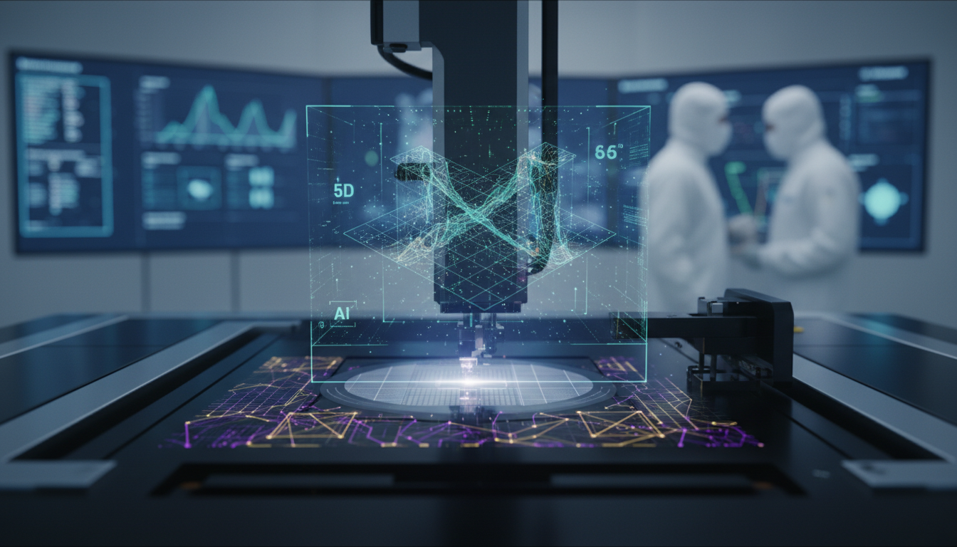
AI Lithography Overlay Tips represent a transformative approach in the Silicon Wafer Engineering sector, leveraging artificial intelligence to enhance overlay precision in lithography processes. This concept encompasses the application of advanced algorithms and machine learning techniques to optimize the alignment of patterns on silicon wafer s, which is critical for the manufacturing of semiconductor devices. As industry stakeholders face increasing demands for higher performance and miniaturization, the integration of AI into lithography becomes essential, aligning with a broader shift towards automation and digital transformation in manufacturing practices.
The significance of the Silicon Wafer Engineering ecosystem is magnified by the implementation of AI Lithography Overlay Tips, as they redefine competitive dynamics and innovation cycles. AI-driven methodologies are fostering enhanced efficiency, enabling faster decision-making, and reshaping interactions among stakeholders. While the promise of improved operational capabilities is substantial, challenges such as integration complexity and evolving expectations present hurdles that must be navigated. Nonetheless, the ongoing adoption of AI technologies opens avenues for growth, encouraging participants to rethink strategies and capitalize on emerging opportunities.
Maximize AI Potential in Lithography Overlay Strategies
Silicon Wafer Engineering companies should strategically invest in AI-driven lithography overlay technologies and forge partnerships with AI specialists to enhance precision and efficiency. This focus on AI integration is expected to yield significant improvements in production quality, reduce costs, and create a sustainable competitive edge in the market.
Transforming Silicon Wafer Engineering: The Role of AI Lithography Overlay Tips
Implementation Framework
Evaluate existing data sources for AI
Deploy optimized AI lithography solutions
Upskill teams on AI tools and techniques
Track AI system effectiveness and accuracy
Optimize workflows based on AI insights
Ensure that all data utilized in AI lithography processes is accurate, complete, and relevant. High-quality data supports better model training, leading to improved overlay accuracy and operational efficiency in silicon wafer engineering .
Technology Partners
Integrate AI-driven models designed for lithography overlay into existing systems. These models enhance precision in the wafer fabrication process, reducing defects and optimizing yield, which is crucial for competitive advantage.
Internal R&D
Conduct comprehensive training programs to ensure that staff are proficient in using AI lithography tools. Skilled personnel can leverage technology effectively, maximizing the benefits and improving overall operational performance.
Industry Standards
Regularly evaluate the performance of AI lithography systems through key performance indicators. Continuous monitoring helps identify areas for improvement, ensuring that the overlay processes meet quality standards and operational goals.
Cloud Platform
Use insights gained from AI analyses to refine lithography processes, enhancing workflow efficiency and product quality. This iterative approach allows for the continuous adaptation of operations to meet evolving industry standards.
Industry Experts
Best Practices for Automotive Manufacturers
Integrate AI Algorithms Seamlessly
- Impact : Enhances defect detection accuracy significantly
Example : Example: In a silicon wafer fabrication plant, an AI algorithm analyzes overlay data in real time, increasing defect detection accuracy by 30% compared to traditional methods, ensuring higher yield and quality in the final product. - Impact : Reduces production downtime and costs
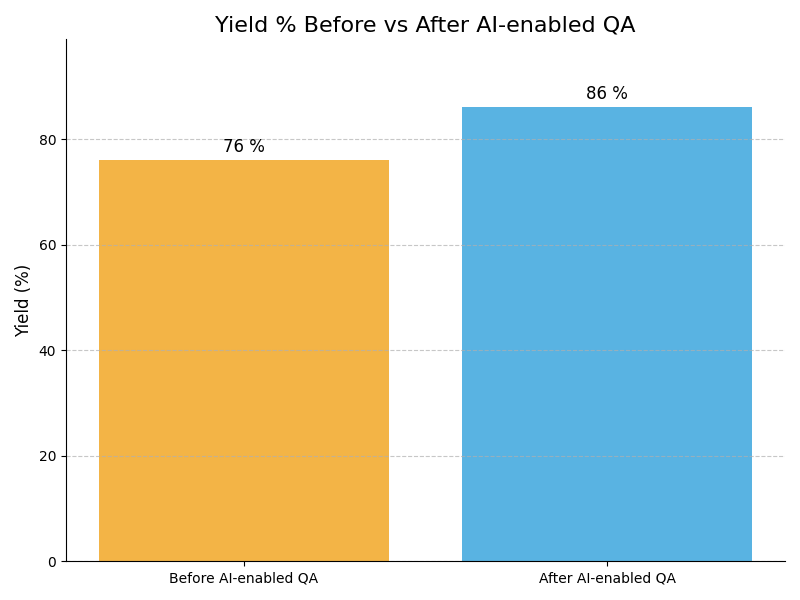
Example : Example: An AI system optimizes the lithography process by predicting equipment failures, leading to a 25% reduction in production downtime, which directly translates into significant cost savings for the facility. - Impact : Improves yield rates and product quality
Example : Example: A semiconductor manufacturer implements AI to enhance yield rates by analyzing defect patterns, resulting in a 15% improvement in product quality and reducing waste during production. - Impact : Accelerates time-to-market for new products
Example : Example: An AI-driven lithography system decreases the time-to-market for new chip designs by optimizing processing steps, allowing a company to launch products 20% faster than competitors.
- Impact : High initial investment for implementation
Example : Example: A leading semiconductor firm faced delays in AI adoption after discovering that the cost of integrating advanced cameras and AI software exceeded initial budget estimates, causing project cancellations. - Impact : Potential data privacy concerns
Example : Example: AI systems in a wafer fabrication plant inadvertently collect sensitive production data, raising alarms about compliance with data privacy regulations and leading to audits and penalties. - Impact : Integration challenges with legacy systems
Example : Example: A manufacturer struggled to integrate AI with outdated machinery, resulting in project setbacks as engineers had to create custom solutions for data transfer, delaying implementation by several months. - Impact : Need for continuous data quality assurance
Example : Example: A dust accumulation issue caused an AI inspection system to misidentify functional wafers as defective, leading to increased scrap rates and the need for frequent recalibration to maintain data accuracy.
Utilize Advanced Data Analytics
- Impact : Identifies critical process inefficiencies
Example : Example: A silicon wafer manufacturer employs advanced data analytics to pinpoint inefficiencies in the lithography process, resulting in a 20% increase in production efficiency and substantial cost reductions. - Impact : Enables predictive maintenance strategies
Example : Example: By analyzing historical data, an AI system predicts maintenance needs for lithography equipment, preventing unplanned downtimes and saving the company thousands in emergency repairs. - Impact : Enhances overall production throughput
Example : Example: A semiconductor plant uses real-time data analytics to enhance throughput, leading to a 30% increase in production capacity without additional resource expenditure. - Impact : Facilitates data-driven decision-making
Example : Example: Data-driven insights from AI empower managers to make informed decisions regarding resource allocation, improving operational effectiveness and strategic planning outcomes.
- Impact : Data integration complexities across systems
Example : Example: A leading semiconductor company experienced integration issues when attempting to unify data from multiple legacy systems, causing delays in AI project timelines and increased costs due to manual data entry. - Impact : Dependence on high-quality training datasets
Example : Example: An AI model trained on outdated datasets produced misleading results, leading to incorrect operational decisions and significant financial losses for a wafer fabrication plant. - Impact : Inaccurate predictions from algorithmic bias
Example : Example: An AI algorithm exhibited bias in its predictions, causing a mismatch between expected and actual production outputs, which led to increased scrap rates and quality control issues. - Impact : Resistance to change from workforce
Example : Example: Employees in a production facility resisted the adoption of AI-based solutions, fearing job losses, which hampered the successful implementation and integration of new technologies.
Train Workforce Continuously
- Impact : Builds essential AI skill sets
Example : Example: A silicon wafer manufacturer invests in continuous training programs for employees, equipping them with AI skill sets that lead to smoother transitions during technology upgrades, significantly enhancing team productivity. - Impact : Fosters a culture of innovation
Example : Example: By fostering a culture of innovation through regular workshops, a semiconductor firm encourages employees to share ideas, resulting in several successful AI-driven process improvements across the organization. - Impact : Increases employee engagement and retention
Example : Example: An AI training initiative improved employee engagement levels at a fabrication plant, reducing turnover rates by 15% as staff felt more invested in their roles and the company's future. - Impact : Enhances adaptability to new technologies
Example : Example: Regular training on emerging AI technologies enables teams to adapt quickly to changes, ensuring that the firm remains competitive in a rapidly evolving market.
- Impact : Training costs can be substantial
Example : Example: A mid-sized semiconductor company faced budget overruns due to unexpected training costs for its workforce, limiting funds available for other critical AI implementation projects. - Impact : Potential knowledge gaps among staff
Example : Example: After a training program, some staff still struggled with new AI tools , resulting in uneven skill levels across teams and impacting overall project performance. - Impact : Resistance to adopting new skills
Example : Example: Employees expressed reluctance to adopt AI technologies, fearing that learning new skills would be overwhelming, which delayed project timelines and reduced overall effectiveness. - Impact : Training effectiveness can vary widely
Example : Example: A training program's effectiveness varied significantly among employees, leading to inconsistencies in AI tool usage and varying levels of productivity across different production lines.
Implement Real-time Monitoring Systems
- Impact : Detects anomalies instantly during production
Example : Example: A silicon wafer production line utilizes real-time monitoring systems to detect deviations during lithography, allowing operators to correct issues instantly, which reduces defect rates by 20%. - Impact : Improves response times for corrective actions
Example : Example: By implementing an AI-driven monitoring system, a semiconductor facility improved its reaction time to equipment anomalies, reducing downtime by 30% and enhancing overall operational efficiency. - Impact : Enhances overall equipment effectiveness
Example : Example: Real-time monitoring enables a semiconductor plant to track equipment effectiveness, leading to a 25% increase in uptime and significant cost reductions in maintenance operations. - Impact : Reduces operational risks significantly
Example : Example: An AI monitoring system identifies potential risks in the production process, allowing teams to implement preventive measures, significantly reducing incidents of equipment failure.
- Impact : High costs associated with technology upgrades
Example : Example: A semiconductor manufacturer faced high costs when upgrading to advanced monitoring technologies, impacting budgets for other essential operations and project developments. - Impact : Data overload complicates decision-making
Example : Example: With the introduction of extensive data from monitoring systems, staff found it challenging to sift through information, leading to decision-making delays and missed opportunities in production adjustments. - Impact : Requires ongoing system maintenance
Example : Example: An AI monitoring system required frequent maintenance, leading to unanticipated costs and operational interruptions as teams scrambled to keep systems online during peak production times. - Impact : Integration with existing processes may falter
Example : Example: Integration challenges arose when the new monitoring system did not mesh well with existing processes, causing temporary disruptions and confusion among production staff during the transition.
Enhance Collaboration Across Teams
- Impact : Improves information sharing among departments
Example : Example: A semiconductor company established cross-functional teams that improved information sharing, leading to a 20% reduction in project cycle times and enhanced collaborative decision-making. - Impact : Accelerates innovation through teamwork
Example : Example: By fostering collaboration between engineering and production teams, a silicon wafer manufacturer accelerated innovation efforts, resulting in the successful launch of two new AI-driven products within a year. - Impact : Enables faster problem resolution
Example : Example: Regular collaboration meetings allowed teams to address production issues promptly, reducing time spent on problem resolution by 30% and enhancing workflow efficiency. - Impact : Enhances project transparency and accountability
Example : Example: Transparent communication across teams improved accountability, allowing for more efficient project tracking and timely adjustments to production schedules, ultimately boosting overall productivity.
- Impact : Miscommunication can lead to errors
Example : Example: Miscommunication between engineering and production teams resulted in a costly error during the lithography process, leading to a significant waste of resources and time in rectifying the issue. - Impact : Team conflicts may arise during projects
Example : Example: Conflicts arose within a cross-functional team during a high-stakes AI project, delaying progress and causing frustration among team members, ultimately impacting project deadlines. - Impact : Collaboration tools can be underutilized
Example : Example: A new collaboration tool implemented in a semiconductor firm saw low adoption rates, leading to missed opportunities for efficient teamwork and information sharing across departments. - Impact : Time-consuming coordination efforts required
Example : Example: Coordinating schedules for cross-departmental meetings consumed valuable time, diverting attention from critical project tasks and slowing down overall progress toward objectives.
Optimize Lithography Parameters
- Impact : Maximizes overlay accuracy and precision
Example : Example: A silicon wafer fabrication facility optimized lithography parameters using AI, achieving a 15% improvement in overlay accuracy, which significantly reduced defects and rework in the production line. - Impact : Reduces waste in production processes
Example : Example: By fine-tuning lithography settings, a semiconductor manufacturer reduced material waste by 20%, translating to substantial cost savings and improved sustainability in operations. - Impact : Enables faster cycle times
Example : Example: Lithography parameter optimization led to a 10% decrease in cycle times within production, enabling faster delivery of products to market and improving customer satisfaction levels. - Impact : Enhances overall product reliability
Example : Example: Enhanced overlay precision resulted in improved product reliability, allowing a semiconductor firm to confidently extend warranty periods on their products, enhancing brand reputation.
- Impact : Over-optimization can lead to diminishing returns
Example : Example: A semiconductor company experienced diminishing returns from over-optimizing lithography parameters, leading to increased defect rates and necessitating a return to previous settings for stability. - Impact : Requires extensive testing and validation
Example : Example: Extensive testing to validate lithography parameter changes delayed production schedules, causing a backlog in orders and impacting customer satisfaction due to late deliveries. - Impact : Potential for increased complexity in processes
Example : Example: Introducing complex optimization algorithms increased the difficulty of the lithography process, leading to operational challenges that slowed down production and required additional training. - Impact : Staff may be resistant to changes
Example : Example: Employees expressed reluctance to adapt to new lithography parameter changes, fearing that their previous expertise would become obsolete, which hampered the implementation of new standards.
AI is revolutionizing semiconductor manufacturing by enabling the production of the most advanced AI chips on US soil through partnerships like ours with TSMC, marking the start of a new industrial era in wafer fabrication.
– Jensen Huang, CEO of NVIDIACompliance Case Studies


Harness AI-driven lithography overlay tips to transform your processes and stay ahead in the competitive Silicon Wafer Engineering landscape. Act fast to lead the change!
Take Test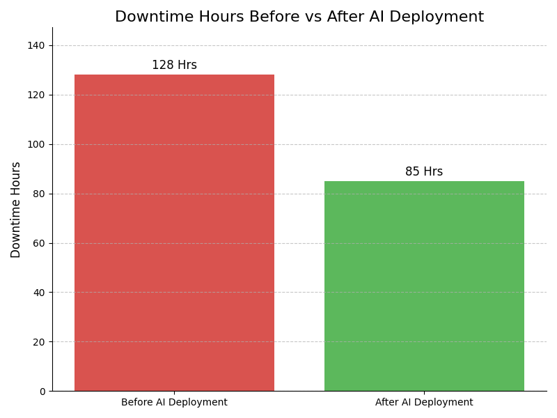
Leadership Challenges & Opportunities
Data Alignment Issues
Utilize AI Lithography Overlay Tips to enhance data consistency across multiple wafer fabrication stages. Implement real-time data synchronization and automated validation processes to ensure accurate overlay measurements. This approach minimizes errors, leading to improved yield and reduced rework costs in production.
Resistance to AI Adoption
Address cultural resistance to AI Lithography Overlay Tips by fostering a collaborative environment. Conduct workshops demonstrating AI benefits, engage stakeholders in pilot projects, and showcase success stories. Such initiatives build trust, promote buy-in, and create a culture of innovation within the Silicon Wafer Engineering team.
High Implementation Costs
Mitigate high costs of AI Lithography Overlay Tips by leveraging cloud-based solutions with flexible pricing models. Start with pilot programs focused on high-impact areas to demonstrate ROI. This phased approach allows incremental investment and validation, paving the way for broader implementation without overwhelming budgets.
Evolving Compliance Standards
Employ AI Lithography Overlay Tips to stay ahead of evolving compliance standards in Silicon Wafer Engineering. Integrate adaptive compliance features that automatically update processes according to new regulations. This proactive strategy minimizes risk, enhances operational efficiency, and ensures consistent adherence across production lines.
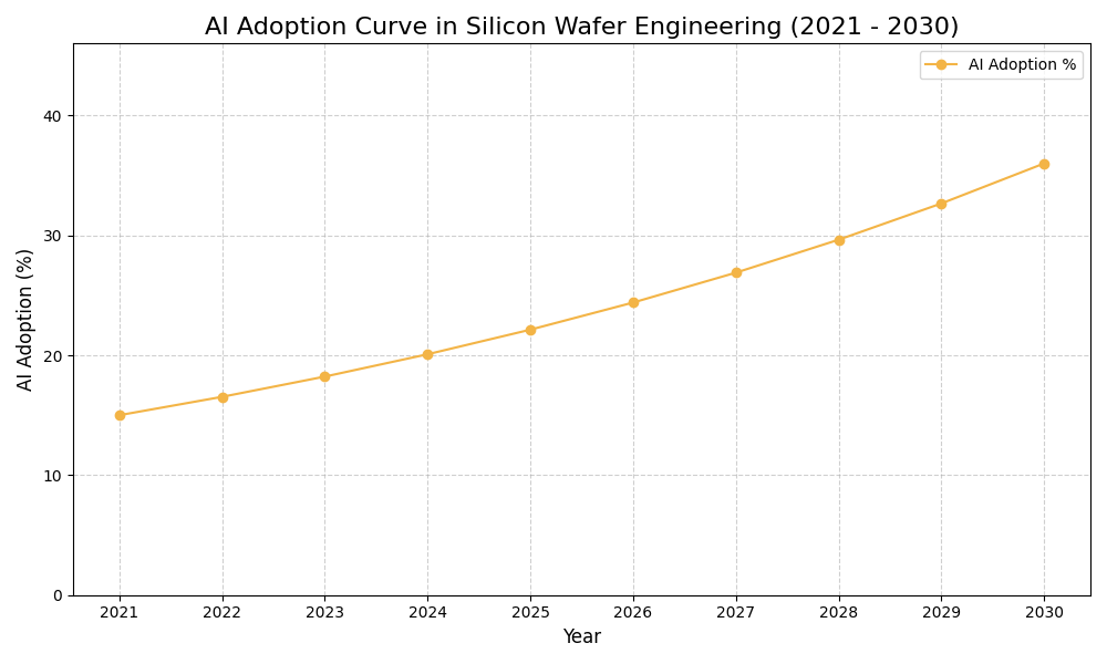
Assess how well your AI initiatives align with your business goals
AI Adoption Graph
AI Use Case vs ROI Timeline
| AI Use Case | Description | Typical ROI Timeline | Expected ROI Impact |
|---|---|---|---|
| Predictive Maintenance for Lithography | AI analyzes equipment data to predict failures, reducing downtime. For example, a semiconductor manufacturer uses AI algorithms to forecast maintenance needs, ensuring lithography machines operate at peak efficiency, thus minimizing costly interruptions. | 6-12 months | High |
| Defect Detection Automation | Utilizing AI for real-time defect detection enhances quality control. For example, an advanced lithography facility employs machine learning to automatically identify and classify defects on silicon wafers, drastically improving yield rates and reducing manual inspections. | 6-9 months | Medium-High |
| Process Optimization | AI algorithms optimize lithography parameters, enhancing output quality. For example, a company integrates AI to fine-tune exposure settings in real time, resulting in improved overlay accuracy and reduced waste during production. | 12-18 months | Medium |
| Supply Chain Efficiency | AI streamlines supply chain management for lithography materials. For example, a manufacturer uses AI to analyze supply chain data, predicting material needs and optimizing inventory levels, thereby minimizing delays and costs. | 6-12 months | Medium-High |
Glossary
Work with Atomic Loops to architect your AI implementation roadmap — from PoC to enterprise scale.
Contact NowFrequently Asked Questions
- AI Lithography Overlay enhances precision in semiconductor manufacturing through advanced algorithms.
- It significantly improves overlay accuracy, crucial for multi-layer chip fabrication.
- The technology reduces defects and minimizes rework, leading to cost savings.
- AI-driven insights enable faster problem-solving and decision-making processes.
- Overall, it positions companies to compete effectively in a rapidly evolving market.
- Begin with a thorough assessment of your current lithography processes and technologies.
- Identify key objectives and success metrics to guide your AI implementation journey.
- Engage stakeholders early to ensure alignment and resource allocation.
- Consider pilot programs to test AI solutions on a smaller scale before full deployment.
- Partnering with AI experts can facilitate smoother integration into existing systems.
- Companies experience enhanced yield rates and improved overall equipment effectiveness.
- AI solutions provide actionable insights, leading to data-driven operational improvements.
- Reduced cycle times result in faster product time-to-market and increased competitiveness.
- Cost savings stem from decreased material waste and optimized resource usage.
- The technology enables continuous improvement through iterative learning and adaptation.
- Common obstacles include resistance to change from staff and existing workflow disruptions.
- Data quality and availability can hinder AI solution effectiveness; thus, proper data management is crucial.
- Integration with legacy systems may pose technical challenges requiring expert guidance.
- Training and upskilling staff are essential to ensure effective AI utilization.
- Adopting a phased approach helps manage risks and allows for adjustments during implementation.
- Organizations should consider implementing AI when they are ready to upgrade existing processes.
- Timing is critical; aligning AI adoption with strategic business goals enhances effectiveness.
- Phased implementations can be beneficial during product development cycles or technology refreshes.
- Regular market assessments help identify competitive pressures that necessitate timely AI adoption.
- Engaging in continuous improvement initiatives can also signal readiness for AI integration.
- AI can optimize alignment processes, crucial for multi-layer semiconductor devices.
- It enables predictive maintenance, reducing downtime and enhancing operational efficiency.
- AI-driven analytics can assist in meeting stringent industry regulatory standards.
- Applications include real-time monitoring and adjustment of lithography parameters during production.
- These technologies support the development of next-generation semiconductor manufacturing techniques.
- Initial investment includes software, hardware, and potential training requirements for staff.
- Long-term savings can offset initial costs through improved efficiency and reduced waste.
- Consider total cost of ownership, including maintenance and upgrade expenses over time.
- Budgeting for pilot programs allows for lower-risk initial investments in AI solutions.
- Evaluating ROI from implemented AI strategies is essential for ongoing investment justification.
- Investing in AI enhances competitive advantage by driving innovation and efficiency.
- It allows for precision improvements, which are crucial for high-stakes semiconductor production.
- AI capabilities can adapt to market changes, ensuring long-term sustainability.
- The technology fosters a culture of data-driven decision-making across the organization.
- Ultimately, this investment positions companies for future success in an evolving industry landscape.