
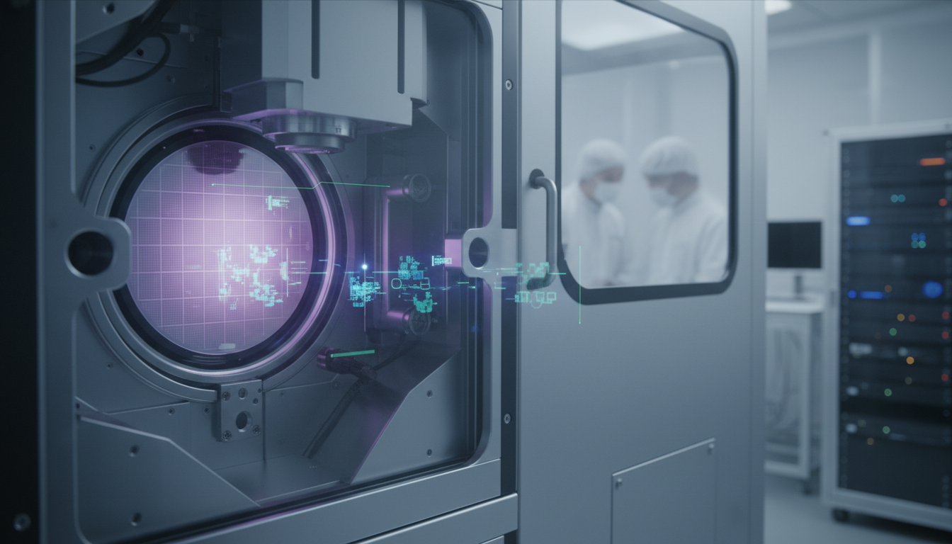
AI Defect Classify SEM Vision
AI Defect Classify SEM Vision represents a transformative approach in the Silicon Wafer Engineering sector, leveraging artificial intelligence to enhance defect classification through scanning electron microscopy (SEM). This innovative framework not only improves accuracy in detecting imperfections but also streamlines the workflows associated with wafer production . As stakeholders increasingly prioritize quality and precision, the relevance of this technology escalates, aligning seamlessly with the broader trend of AI adoption across various operational paradigms.
The ecosystem surrounding Silicon Wafer Engineering is evolving rapidly due to the integration of AI-driven practices. These advancements are reshaping competitive dynamics and accelerating innovation cycles, fostering more effective interactions among stakeholders. The adoption of AI not only enhances operational efficiency but also refines decision-making processes, paving the way for long-term strategic benefits. However, organizations must navigate challenges such as integration complexity and shifting expectations, while also seizing growth opportunities that arise from this technological shift.
Action to Take --- Drive AI Innovations in Defect Classification
Silicon Wafer Engineering companies should strategically invest in AI Defect Classify SEM Vision technologies and form partnerships with leading AI firms to enhance defect detection and classification capabilities. Implementing these AI solutions is expected to significantly improve yield rates, reduce production costs, and strengthen competitive advantages in the market.
How AI is Revolutionizing Defect Classification in Silicon Wafer Engineering
Implementation Framework
Combine relevant data for AI training
Refine AI models for accuracy
Utilize AI for defect detection
Equip teams with AI skills
Gather and integrate manufacturing data from various sources to enhance AI model training. This ensures comprehensive datasets for defect classification, boosting accuracy and operational efficiency in Silicon Wafer Engineering .
Internal R&D
Continuously optimize AI algorithms by employing machine learning techniques to reduce false positives in defect classification. This significantly improves decision-making efficiency and minimizes production costs in wafer engineering operations.
Technology Partners
Deploy real-time monitoring systems using AI to identify defects during the manufacturing process. This proactive approach enhances quality control and reduces the need for extensive post-production inspections in wafer engineering .
Industry Standards
Train workforce on AI tools and technologies to enable effective usage of AI-driven defect classification. This empowers employees and fosters a culture of continuous improvement in Silicon Wafer Engineering practices.
Cloud Platform
Best Practices for Automotive Manufacturers
Integrate AI Algorithms Effectively
- Impact : Enhances defect detection accuracy significantly
Example : Example: In a semiconductor fabrication plant, an AI algorithm identifies defects on silicon wafers with 95% accuracy, reducing manual inspection time by 50% and increasing throughput. - Impact : Reduces production downtime and costs
Example : Example: A leading chip manufacturer implemented AI for real-time defect detection, which decreased production downtime by 30%, saving costs and increasing overall yield. - Impact : Improves quality control standards
Example : Example: An advanced manufacturing facility upgraded its quality control with AI, ensuring that 99% of defective wafers were caught before reaching the final testing phase. - Impact : Boosts overall operational efficiency
Example : Example: AI-enabled monitoring systems dynamically adjust parameters during production, maintaining optimal operational efficiency and reducing waste during peak hours.
- Impact : High initial investment for implementation
Example : Example: A semiconductor company postponed its AI deployment after discovering that the required hardware upgrades would exceed budget limits, delaying expected ROI. - Impact : Potential data privacy concerns
Example : Example: During an AI pilot program, sensitive production data was inadvertently collected, raising concerns about compliance with data protection regulations. - Impact : Integration challenges with existing systems
Example : Example: An AI system designed for defect classification struggled to integrate with legacy equipment, causing delays in deployment and increased operational costs. - Impact : Dependence on continuous data quality
Example : Example: A factory faced issues when inconsistent data quality led to misclassifications, resulting in increased scrap rates and the need for manual inspections.
Utilize Real-time Monitoring
- Impact : Improves immediate defect identification
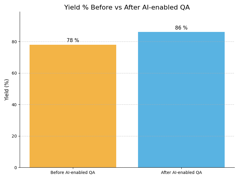
Example : Example: A silicon wafer manufacturer implemented real-time AI monitoring, which enabled immediate identification of defects, resulting in a 40% increase in first-pass yield and reducing rework costs significantly. - Impact : Facilitates rapid corrective actions
Example : Example: By integrating AI into their monitoring systems, a semiconductor plant achieved rapid corrective actions, cutting down production delays caused by defects by 35% and improving overall productivity. - Impact : Enhances overall production quality
Example : Example: An advanced semiconductor facility utilized AI for real-time defect monitoring, enhancing production quality metrics by catching 90% of defects before reaching critical stages of fabrication. - Impact : Reduces waste through early detection
Example : Example: A manufacturer employed AI-driven monitoring to identify defects early, reducing material waste by 25% and contributing to sustainable production practices.
- Impact : Requires extensive data collection infrastructure
Example : Example: A wafer fabrication plant invested heavily in data collection infrastructure but faced challenges integrating with existing systems, resulting in underutilized AI capabilities and wasted resources. - Impact : Potential for false positives and negatives
Example : Example: An AI monitoring system generated false positives, leading to unnecessary inspections and production delays that frustrated operators and increased costs. - Impact : Increased operational complexity
Example : Example: Increased operational complexity from AI integration led to confusion among staff, resulting in errors during the production process and a temporary drop in output. - Impact : Dependence on AI system reliability
Example : Example: A semiconductor manufacturer faced reliability issues with their AI system, which led to significant downtime during critical production cycles, impacting delivery schedules and customer satisfaction.
Train Workforce Regularly
- Impact : Enhances AI system utilization
Example : Example: A semiconductor company launched continuous training programs for employees on AI tools, resulting in a 50% increase in system utilization and better alignment with production goals. - Impact : Improves team adaptability to technology
Example : Example: By regularly training staff on AI technologies, a silicon wafer manufacturer improved adaptability, enabling teams to respond effectively to emerging challenges and trends. - Impact : Fosters a culture of innovation
Example : Example: A culture of innovation flourished in a semiconductor plant after implementing ongoing AI training, leading to new ideas that enhanced production processes and efficiency. - Impact : Reduces resistance to change
Example : Example: Regular training sessions helped reduce resistance to AI adoption within teams, leading to smoother transitions and improved morale in a rapidly evolving technological landscape.
- Impact : Training costs can be substantial
Example : Example: A silicon wafer manufacturer incurred substantial costs associated with extensive AI training programs, impacting short-term budgets and causing financial strain on other initiatives. - Impact : Knowledge retention may vary among staff
Example : Example: Knowledge retention varied significantly among staff after AI training, leading to inconsistent utilization of the systems and varying levels of efficiency across teams. - Impact : Potentially limited training resources
Example : Example: A company faced challenges due to limited training resources, which hindered the effectiveness of their AI integration efforts and slowed overall progress. - Impact : Resistance from non-technical staff
Example : Example: Non-technical staff expressed resistance to AI training, creating barriers to adoption that delayed project timelines and reduced overall productivity in the facility.
Implement Feedback Loops
- Impact : Facilitates continuous improvement
Example : Example: A semiconductor plant established feedback loops, enabling real-time data input into AI systems, leading to a 20% improvement in algorithm accuracy over six months. - Impact : Enhances AI algorithm accuracy
Example : Example: By creating a structured feedback mechanism, an AI defect classification system at a silicon wafer manufacturer became more adaptive, improving defect detection rates by 30% during production. - Impact : Encourages employee engagement
Example : Example: Employee engagement increased significantly when staff could provide insights into AI performance, resulting in novel solutions that optimized defect classification processes and improved outcomes. - Impact : Optimizes defect classification processes
Example : Example: Implementing feedback loops allowed for constant optimization of defect classification processes, which enhanced the overall quality of the final products and reduced scrap rates.
- Impact : Requires commitment from all stakeholders
Example : Example: A semiconductor manufacturer struggled to get buy-in from all stakeholders for feedback loops, resulting in missed opportunities for improvements and stagnated progress. - Impact : Potential for feedback overload
Example : Example: Feedback overload became an issue in a silicon wafer facility , where too much data confused decision-makers and led to delays in effective actions being taken. - Impact : Implementation can be time-consuming
Example : Example: Implementation of feedback loops took longer than anticipated, causing delays in the expected benefits of AI integration and frustrating team members eager for results. - Impact : Dependence on staff participation
Example : Example: Dependence on staff participation in providing feedback created bottlenecks, as some employees were reluctant to share insights, limiting the effectiveness of the feedback system.
Leverage Data Analytics
- Impact : Enables data-driven decision-making
Example : Example: A silicon wafer manufacturer utilized data analytics to inform decision-making, leading to a 25% reduction in defects based on actionable insights derived from production data. - Impact : Identifies trends in defect occurrence
Example : Example: By analyzing defect occurrence trends over time, a semiconductor plant was able to implement targeted interventions, decreasing defect rates by 15% across key processes. - Impact : Optimizes resource allocation
Example : Example: Data analytics allowed a facility to optimize resource allocation, ensuring that inspection resources were focused on areas with the highest defect rates, improving overall efficiency. - Impact : Enhances strategic planning capabilities
Example : Example: Enhanced strategic planning was achieved when a semiconductor manufacturer used data analytics to forecast production challenges, allowing timely adjustments that minimized disruptions.
- Impact : Requires robust data management systems
Example : Example: A semiconductor company faced challenges in managing data due to inadequate systems, resulting in lost insights and missed opportunities for improvements in defect classification. - Impact : Data analysis may introduce biases
Example : Example: Biases in data analysis led a silicon wafer manufacturer to overlook critical defect patterns, causing significant issues during the production phase and increased rework costs. - Impact : May overlook smaller, critical defects
Example : Example: Focusing on larger defects during data analysis caused a facility to miss smaller yet critical defects, impacting overall product quality and customer satisfaction. - Impact : Dependence on analytical skill sets
Example : Example: The need for specialized analytical skills created a talent gap in a semiconductor plant, limiting the effectiveness of data-driven decisions and slowing down improvements.
Adopt Collaborative AI Models
- Impact : Enhances teamwork across departments
Example : Example: A silicon wafer engineering team adopted collaborative AI models that facilitated communication between departments, leading to a 30% boost in project delivery speed and improved results. - Impact : Promotes knowledge sharing
Example : Example: By promoting knowledge sharing through collaborative AI initiatives, a semiconductor plant saw significant improvements in collective problem-solving and innovation among teams. - Impact : Increases system adaptability
Example : Example: Collaborative AI models allowed different departments to adapt their processes, resulting in a cohesive approach that improved operational efficiency and reduced time to market. - Impact : Facilitates cross-functional innovations
Example : Example: Facilitating cross-functional innovations through collaborative AI led to new methods for defect classification, enhancing overall production quality and customer satisfaction.
- Impact : Requires cultural shift within organization
Example : Example: A semiconductor manufacturer struggled with cultural resistance when introducing collaborative AI models, leading to delays in project timelines and missed opportunities for innovation. - Impact : Implementation can be resource-intensive
Example : Example: Resource-intensive implementation of collaborative AI models drained budgets and caused temporary disruptions in day-to-day operations, affecting overall productivity. - Impact : May face resistance from silos
Example : Example: Silos within departments created barriers to effective collaboration, resulting in frustrations and reduced effectiveness of the AI systems across the organization. - Impact : Dependence on effective communication
Example : Example: Dependence on effective communication for collaborative AI initiatives led to misunderstandings and errors, causing setbacks in project execution and reduced efficiency.
Ensure Compliance with Standards
- Impact : Reduces risk of regulatory penalties
Example : Example: A semiconductor company focused on compliance with industry standards, which helped them avoid costly regulatory penalties and maintain a positive reputation in the market. - Impact : Enhances product reliability
Example : Example: By ensuring adherence to standards, a silicon wafer manufacturer enhanced product reliability, leading to a 20% reduction in warranty claims and higher customer satisfaction. - Impact : Improves customer trust and satisfaction
Example : Example: Compliance with regulations fostered customer trust, as a semiconductor firm consistently delivered high-quality products that met all safety and performance standards. - Impact : Facilitates smoother audits and inspections
Example : Example: Smooth audits and inspections became possible for a manufacturing facility by maintaining compliance, resulting in faster turnaround times and less disruption to operations.
- Impact : Compliance processes may be complex
Example : Example: A semiconductor manufacturer faced challenges with complex compliance processes, which slowed down product rollout and increased frustration among teams seeking to innovate. - Impact : Continual updates to regulations required
Example : Example: Constant updates to regulations led to a reactive approach in a silicon wafer facility , resulting in missed opportunities for proactive improvements and innovation. - Impact : Potentially high costs for compliance
Example : Example: High costs associated with compliance measures strained budgets, causing delays in other critical projects and impacting overall operational efficiency. - Impact : Dependence on expert knowledge
Example : Example: Dependence on expert knowledge for compliance management created bottlenecks, as staff turnover led to gaps in understanding of critical regulatory requirements.
The path to a trillion-dollar semiconductor industry requires rethinking how manufacturers leverage data and deploy AI-driven automation to handle unprecedented manufacturing complexity in wafer production and advanced packaging.
– John Kibarian, CEO of PDF SolutionsCompliance Case Studies


Don't let outdated methods hold you back. Embrace AI-driven solutions in SEM Vision to elevate your Silicon Wafer Engineering and outperform the competition.
Take Test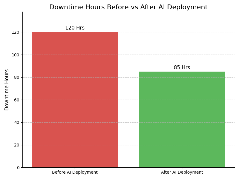
Leadership Challenges & Opportunities
Data Quality Assurance
Utilize AI Defect Classify SEM Vision to standardize data collection processes, ensuring high-quality inputs for analysis. Implement automated data validation checks and feedback loops to continuously improve data integrity. This enhances defect detection accuracy and optimizes decision-making in Silicon Wafer Engineering.
Integration with Legacy Systems
Adopt a modular approach with AI Defect Classify SEM Vision, leveraging APIs for seamless integration with existing systems. Employ phased implementation to minimize disruptions, allowing gradual adoption while maintaining operational integrity. This strategy ensures compatibility and enhances overall system efficiency.
High Implementation Costs
Leverage AI Defect Classify SEM Vision through cloud-based solutions that reduce initial capital outlay. Focus on cost-effective pilot projects targeting high-impact areas to demonstrate ROI. Gradual scaling based on proven success can secure additional funding and minimize financial risks in Silicon Wafer operations.
Talent Acquisition Challenges
Deploy AI Defect Classify SEM Vision alongside targeted recruitment initiatives to attract specialized talent. Partner with educational institutions for training programs focused on AI in semiconductor technologies. This builds a skilled workforce while fostering innovation and aligning talent with industry needs.
Assess how well your AI initiatives align with your business goals
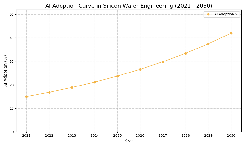
AI Adoption Graph
AI Use Case vs ROI Timeline
| AI Use Case | Description | Typical ROI Timeline | Expected ROI Impact |
|---|---|---|---|
| Defect Detection Automation | AI automates the identification of defects in silicon wafers, enhancing precision in manufacturing. For example, using SEM vision, a semiconductor company improved defect detection rates by 30%, reducing waste and rework costs significantly. | 6-12 months | High |
| Quality Assurance Enhancement | Integrating AI in quality assurance processes helps in real-time monitoring and analysis of silicon wafers. For example, an AI system flagged anomalies during production, allowing for immediate corrective actions, thus improving overall product quality. | 12-18 months | Medium-High |
| Predictive Maintenance Scheduling | AI algorithms analyze equipment data to predict maintenance needs, minimizing downtime. For example, a silicon wafer manufacturer implemented predictive maintenance, reducing unexpected breakdowns by 40% and enhancing production efficiency. | 12-18 months | Medium |
| Yield Optimization | AI analyzes production data to optimize yields, ensuring maximum output with minimal defects. For example, a semiconductor plant utilized AI to adjust processes dynamically, achieving a 15% increase in yield rates over six months. | 6-12 months | High |
Glossary
Work with Atomic Loops to architect your AI implementation roadmap — from PoC to enterprise scale.
Contact NowFrequently Asked Questions
- AI Defect Classify SEM Vision identifies defects using advanced image analysis techniques.
- It improves quality control by automating defect detection processes in semiconductor manufacturing.
- This technology enhances precision, reducing manual inspection errors significantly.
- Organizations benefit from faster detection, enabling quicker response to production issues.
- Ultimately, it leads to improved product quality and operational efficiency in wafer fabrication.
- Integration begins with assessing current systems and identifying suitable AI tools.
- Collaboration with IT teams ensures smooth compatibility with existing infrastructure.
- Training staff on new technology is crucial for successful adoption and implementation.
- Data migration and testing phases are vital for ensuring system reliability.
- Continuous monitoring post-integration helps optimize performance and address challenges.
- AI significantly enhances detection accuracy, minimizing false positives and negatives.
- It leads to reduced cycle times, allowing for faster production rates and deliveries.
- Organizations can achieve substantial cost savings through automation of manual processes.
- AI-driven insights support data-driven decisions, improving overall operational strategies.
- Competitive advantages arise from enhanced product quality and customer satisfaction.
- Common obstacles include resistance to change from employees accustomed to traditional methods.
- Data quality issues can hinder AI performance, necessitating thorough data cleansing.
- Integration with legacy systems poses technical challenges requiring expert intervention.
- Organizational readiness is a critical factor influencing successful implementation.
- Establishing a clear strategy and addressing concerns can mitigate these challenges.
- Organizations should consider adoption when facing increasing defect rates and quality issues.
- Timing is ideal during technology upgrades or when scaling production capabilities.
- Assessing the maturity of current processes can indicate readiness for AI integration.
- Proactive planning helps align AI initiatives with business goals and objectives.
- Continuous innovation in the industry further emphasizes the need for timely adoption.
- Adhering to industry benchmarks ensures compliance and enhances product reliability.
- Standards focus on quality assurance, data handling, and process efficiency.
- Regular audits and assessments are crucial to maintain compliance with evolving standards.
- Collaboration with regulatory bodies can streamline adherence to industry requirements.
- Staying informed about emerging standards helps organizations remain competitive.
- Investing now positions organizations as leaders in quality and operational excellence.
- Early adoption can lead to significant cost reductions and efficiency gains.
- Improved defect detection enhances customer trust and loyalty in the long term.
- AI technology is rapidly evolving, and early investment maximizes competitive advantage.
- Long-term benefits include sustained innovation and market responsiveness.