
AI Contam Source Finder
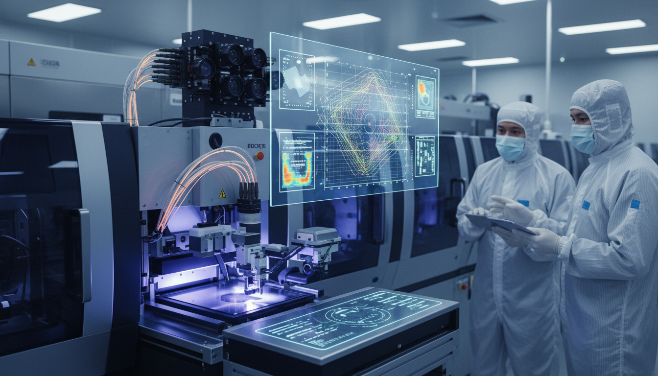
In the realm of Silicon Wafer Engineering, the "AI Contam Source Finder" represents a transformative approach to identifying contamination sources that can compromise wafer integrity. This innovative concept leverages artificial intelligence to enhance detection methodologies, leading to more precise diagnostics and streamlined operational processes. As the industry increasingly prioritizes quality control and efficiency, the relevance of this technology becomes paramount, aligning seamlessly with the ongoing AI-led transformations that redefine operational and strategic priorities across the sector.
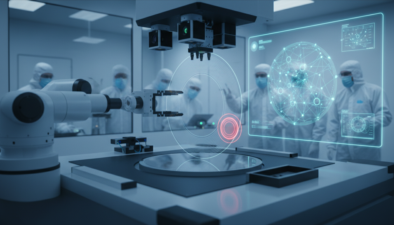
The Silicon Wafer Engineering ecosystem is experiencing a paradigm shift, where AI-driven practices are reshaping competitive dynamics and fostering rapid innovation cycles. The integration of AI not only enhances decision-making capabilities but also influences the strategic direction of stakeholders by improving operational efficiency and transparency. While the adoption of such advanced technologies presents growth opportunities, it also brings challenges, including integration complexity and evolving expectations. Navigating these dynamics will be critical for stakeholders aiming to capitalize on the benefits of AI while addressing potential barriers to implementation.
Leverage AI for Contamination Source Identification
Silicon Wafer Engineering companies should strategically invest in partnerships focused on AI technologies to enhance the capabilities of AI Contam Source Finder systems. Implementing these AI-driven solutions is expected to improve defect detection, reduce costs, and create a significant competitive advantage in the market.
How AI is Revolutionizing Silicon Wafer Engineering?
Implementation Framework
Utilize AI to detect contaminants
Leverage AI for predictive analytics
Implement AI-driven surveillance systems
Use AI to refine production settings
Enhance skills for effective AI use
Implement advanced AI algorithms for real-time monitoring of contaminants in silicon wafer production . This enhances yield, reduces waste, and improves overall operational efficiency, ensuring high-quality products and customer satisfaction.
Technology Partners
Employ machine learning techniques to analyze historical contamination data, identifying patterns that predict future occurrences. This proactive approach minimizes disruptions and enhances supply chain resilience in silicon wafer manufacturing processes.
Industry Standards
Develop and deploy AI-powered monitoring systems for continuous assessment of wafer conditions. This integration ensures immediate response to contamination risks, safeguarding production quality and maintaining competitive advantage in the industry.
Cloud Platform
Utilize AI to optimize manufacturing parameters based on contamination data analysis. Adjusting these parameters enhances production efficiency, reduces defects, and aligns processes with industry best practices, maximizing profitability and quality outcomes.
Internal R&D
Conduct training sessions for staff on AI tools and data interpretation to ensure effective utilization. Empowering employees enhances operational capabilities, fosters innovation, and drives continuous improvement in contamination management.
Technology Partners
Best Practices for Automotive Manufacturers
Integrate AI Algorithms Effectively
- Impact : Enhances defect detection accuracy significantly
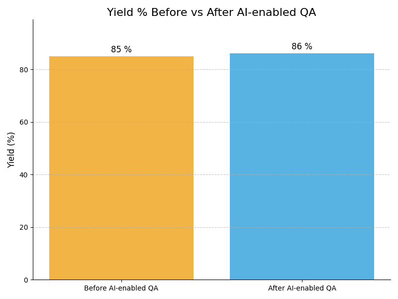
Example : Example: In a semiconductor facility, AI algorithms analyze wafer images , identifying defects that traditional methods miss, leading to a 20% increase in yield during production runs. - Impact : Reduces production downtime and costs
Example : Example: A leading silicon wafer manufacturer implements AI for real-time defect detection, reducing downtime by 15 hours weekly and saving approximately $50,000 in operational costs each month. - Impact : Improves quality control standards
Example : Example: Quality control teams leverage AI to monitor and adjust manufacturing parameters dynamically, ensuring compliance with tight specifications and reducing rejection rates significantly. - Impact : Boosts overall operational efficiency
Example : Example: An AI-driven monitoring system optimizes equipment performance, enhancing throughput by 25%, enabling the facility to meet increasing market demand efficiently.
- Impact : High initial investment for implementation
Example : Example: A mid-sized semiconductor producer hesitates to implement AI due to high upfront costs, including system integration and hardware purchases, which exceed projected budgets. - Impact : Potential data privacy concerns
Example : Example: During an AI deployment, a factory inadvertently collects sensitive employee data, raising compliance issues and delaying the rollout due to privacy law concerns. - Impact : Integration challenges with existing systems
Example : Example: An AI system fails to integrate with legacy manufacturing equipment, requiring costly upgrades and additional resources to bridge the technology gap. - Impact : Dependence on continuous data quality
Example : Example: A silicon wafer production line experiences misclassifications due to inconsistent data quality, resulting in increased scrap rates and operational disruptions.
Utilize Real-time Monitoring
- Impact : Improves defect detection speed
Example : Example: Real-time AI monitoring in a wafer fab detects minute particle contamination, allowing immediate corrective action, which improves yield rates by 30% compared to manual checks. - Impact : Enhances process adjustment capabilities
Example : Example: A leading silicon wafer manufacturer employs AI to adjust processing parameters dynamically, resulting in a 20% reduction in cycle time and increased throughput. - Impact : Supports data-driven decision making
Example : Example: Data-driven insights from real-time monitoring enable managers to make informed decisions, leading to a 15% reduction in waste materials during production. - Impact : Increases overall production efficiency
Example : Example: An AI system continuously analyzes production data, enhancing operational efficiency and boosting output by 10% during peak manufacturing periods.
- Impact : Dependence on robust IT infrastructure
Example : Example: A wafer fabrication plant finds its AI monitoring system underperforms due to outdated IT infrastructure, causing delays in production and mismanagement of resources. - Impact : Need for ongoing maintenance and updates
Example : Example: Continuous updates and maintenance of an AI system require dedicated IT personnel, increasing operational costs and diverting resources from core production activities. - Impact : Potential for system errors and misinterpretations
Example : Example: An AI algorithm misinterprets data, leading to false positives in defect detection, causing unnecessary production halts and increased costs for rework. - Impact : Challenges in workforce adaptation
Example : Example: Employees struggle to adapt to AI-driven monitoring systems, leading to resistance and decreased morale as they fear job displacement by technology.
Train Workforce Regularly
- Impact : Enhances employee AI competency
Example : Example: A silicon wafer manufacturer conducts biannual training sessions, resulting in 90% of employees feeling confident in using AI tools, thus boosting productivity by 15%. - Impact : Reduces resistance to AI adoption
Example : Example: Regular AI training reduces employee resistance, allowing smoother integration of AI systems into the workflow, which enhances collaboration and reduces downtime. - Impact : Promotes a culture of innovation
Example : Example: Training encourages employees to innovate, leading to 5 new process improvements that enhance manufacturing efficiency and reduce costs by 10% annually. - Impact : Improves overall operational performance
Example : Example: Continuous learning initiatives improve operational performance, with teams effectively leveraging AI insights, resulting in a 20% increase in production quality over six months.
- Impact : Training costs may exceed budget
Example : Example: A silicon wafer company overspends on extensive training programs, leading to budget overruns that impact other operational investments and project timelines. - Impact : Employee turnover can disrupt training
Example : Example: High employee turnover in a tech department disrupts ongoing AI training, resulting in lost knowledge and decreased productivity in AI utilization. - Impact : Resistance to change from staff
Example : Example: Some staff resist AI integration, leading to a cultural divide within teams and impacting overall project success as they fail to adopt new technologies. - Impact : Potential skill gaps in workforce
Example : Example: A lack of foundational skills in AI among employees creates skill gaps that hinder effective use of advanced AI systems, leading to inefficiencies in operations.
Implement Predictive Analytics
- Impact : Anticipates equipment failures
Example : Example: Predictive analytics in a wafer fab identifies potential equipment failures, allowing preemptive maintenance that reduces unplanned downtime by 30% and saves costs. - Impact : Optimizes maintenance schedules
Example : Example: A silicon wafer manufacturer uses AI to optimize maintenance schedules, resulting in a 15% decrease in maintenance costs and improving overall equipment effectiveness. - Impact : Reduces operational costs
Example : Example: By leveraging predictive analytics, a semiconductor plant enhances production reliability, achieving a 25% reduction in defect rates over three months due to better equipment management. - Impact : Improves production reliability
Example : Example: An AI-driven system forecasts production demands accurately, helping the company adjust resource allocation efficiently, reducing operational costs by 10%.
- Impact : Requires high-quality data inputs
Example : Example: A silicon wafer facility experiences difficulties in applying predictive analytics due to poor data quality, resulting in inaccurate forecasts and operational delays. - Impact : Can be complex to implement
Example : Example: A complex predictive analytics system takes longer to implement than expected, causing disruptions in the production timeline and increased costs. - Impact : May lead to over-reliance on predictions
Example : Example: Over-reliance on predictive analytics leads a manufacturer to overlook human expertise, resulting in missed opportunities for process improvements and innovation. - Impact : Potential for false positives
Example : Example: False positives from predictive analytics create unnecessary maintenance activities, causing production slowdowns and increased operational costs as teams react to inaccuracies.
Leverage AI for Root Cause Analysis
- Impact : Speeds up problem resolution
Example : Example: An AI-powered root cause analysis tool identifies contamination sources in a silicon wafer , reducing investigation time by 50% and improving overall product quality. - Impact : Enhances defect identification accuracy
Example : Example: In a manufacturing environment, AI algorithms accurately pinpoint defects, allowing for rapid corrective actions that enhance product quality and customer satisfaction. - Impact : Improves overall product quality
Example : Example: An AI system continuously analyzes production data, facilitating continuous improvement processes that lead to a 15% reduction in defect rates over six months. - Impact : Facilitates continuous improvement
Example : Example: Speedy identification of root causes using AI helps teams implement solutions quickly, boosting operational efficiency and reducing scrap rates significantly.
- Impact : Requires specialized knowledge for analysis
Example : Example: A silicon wafer manufacturer struggles to interpret complex AI findings, delaying corrective actions and prolonging production issues that could have been resolved. - Impact : Dependence on accurate data collection
Example : Example: Inaccurate data collection undermines AI root cause analysis, leading to misguided conclusions and further production issues, affecting overall yield. - Impact : Potential for misinterpretation of data
Example : Example: Misinterpretation of AI-generated insights leads to inappropriate corrective measures, resulting in increased defect rates and operational disruptions. - Impact : Challenges in integrating findings into processes
Example : Example: Integrating AI findings into existing processes proves challenging, as teams resist changing established methods, hindering productivity and process improvements.
In flip chip or bonded wafers, there is a pressing need for quick, non-destructive inspection to detect voids and particles between bonded surfaces. High-speed infrared imaging addresses this need, providing real-time feedback to enhance throughput.
– Melvin Lee Wei Heng, Senior Manager Applications Engineering at Onto InnovationCompliance Case Studies


Empower your Silicon Wafer Engineering with AI-driven solutions. Transform your processes and outpace competitors by identifying contamination sources swiftly and accurately.
Take Test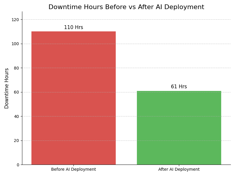
Leadership Challenges & Opportunities
Data Integrity Challenges
Utilize AI Contam Source Finder's advanced algorithms to enhance data accuracy through real-time contamination analysis. Implement automated data cleansing protocols that ensure reliable inputs for decision-making, thus improving overall yield and product quality in Silicon Wafer Engineering.
Complexity in Contamination Detection
Apply AI Contam Source Finder's machine learning capabilities to streamline contamination source identification. By integrating sensor data and historical contamination patterns, the technology can predict and mitigate contamination risks, ensuring higher efficiency and reduced waste in the manufacturing process.
Cultural Resistance to Change
Foster a positive change management strategy by involving employees in the adoption of AI Contam Source Finder. Conduct workshops demonstrating the technology's value, and promote a culture of innovation, which will enhance engagement and acceptance of new methodologies within the Silicon Wafer Engineering team.
High Initial Investment Costs
Leverage AI Contam Source Finder's subscription-based model to lower upfront financial barriers. Begin with pilot projects targeting specific contamination issues to demonstrate ROI. This phased approach allows gradual scaling and investment in additional features once initial successes are validated, optimizing budget utilization.
Assess how well your AI initiatives align with your business goals
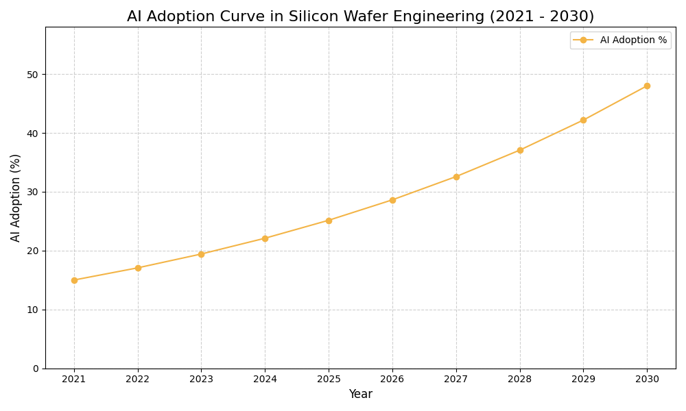
AI Adoption Graph
AI Use Case vs ROI Timeline
| AI Use Case | Description | Typical ROI Timeline | Expected ROI Impact |
|---|---|---|---|
| Real-time Contamination Detection | AI systems can monitor contamination levels in silicon wafer production, identifying issues in real-time to prevent defective products. For example, an AI system can analyze particle counts and alert operators immediately to abnormal levels, ensuring immediate corrective actions. | 6-12 months | High |
| Predictive Maintenance for Equipment | AI can predict equipment failures before they occur, allowing for timely maintenance and reduced downtime. For example, sensors collect data on machinery performance, and AI analyzes this data to forecast when maintenance should be performed, optimizing operational efficiency. | 12-18 months | Medium-High |
| Quality Control Automation | AI can automate the quality inspection process for silicon wafers, ensuring higher accuracy and efficiency. For example, AI-powered imaging systems can quickly identify defects in wafers, reducing the need for manual inspection and speeding up production cycles. | 6-9 months | High |
| Supply Chain Optimization | AI can analyze supply chain data to optimize inventory levels and reduce costs. For example, an AI tool can predict the demand for silicon wafers based on market trends, allowing companies to adjust production schedules and inventory accordingly. | 6-12 months | Medium-High |
Glossary
Work with Atomic Loops to architect your AI implementation roadmap — from PoC to enterprise scale.
Contact NowFrequently Asked Questions
- AI Contam Source Finder enhances contamination detection in semiconductor manufacturing processes.
- It utilizes machine learning to identify sources of contamination effectively and efficiently.
- The tool aids in improving the quality of silicon wafers and reducing defects.
- By leveraging AI, companies can streamline their production workflows significantly.
- This results in lower operational costs and higher product yields for manufacturers.
- Begin by assessing your current contamination management processes for improvement opportunities.
- Engage stakeholders to align on objectives and expected outcomes from AI implementation.
- Pilot projects can be initiated to test the AI technology in controlled environments.
- Ensure you allocate necessary resources, including training for your team on the technology.
- Regularly evaluate progress and make adjustments based on pilot results to optimize deployment.
- Utilizing AI Contam Source Finder leads to significant operational efficiency improvements.
- Companies benefit from reduced contamination rates and enhanced product quality metrics.
- The technology offers insights that inform better decision-making processes.
- Organizations often experience improved return on investment through cost reductions.
- Competitive advantages arise from faster innovation cycles and superior product offerings.
- Resistance to change from staff can hinder the adoption of new AI technologies.
- Integrating AI with existing systems may present technical complexities and challenges.
- Data quality issues can affect the performance and accuracy of the AI tool.
- Budget constraints can limit the scope of implementation and necessary resources.
- Developing a change management strategy can mitigate many of these challenges effectively.
- Organizations should consider implementation when experiencing frequent contamination issues.
- Timing is critical when aiming to enhance quality and production efficiency.
- A readiness assessment can help determine if the infrastructure supports AI tools.
- Market competition may drive the need for faster and more efficient processes.
- Planning ahead ensures that resources are adequately allocated for successful implementation.
- AI Contam Source Finder can be used to monitor contamination in cleanroom environments.
- It aids in identifying sources of defects in wafer fabrication and processing stages.
- Companies can employ the technology for predictive maintenance of manufacturing equipment.
- Regulatory compliance is enhanced through accurate contamination tracking and reporting.
- Adoption of AI can help meet industry benchmarks for quality assurance more effectively.
- Regulatory standards must be adhered to when implementing AI technologies in production.
- Data privacy and protection laws are critical when handling sensitive manufacturing data.
- Documentation and reporting practices should align with industry regulatory requirements.
- Ensuring transparency in AI decision-making processes enhances compliance efforts.
- Regular audits can help maintain compliance and identify areas for improvement.