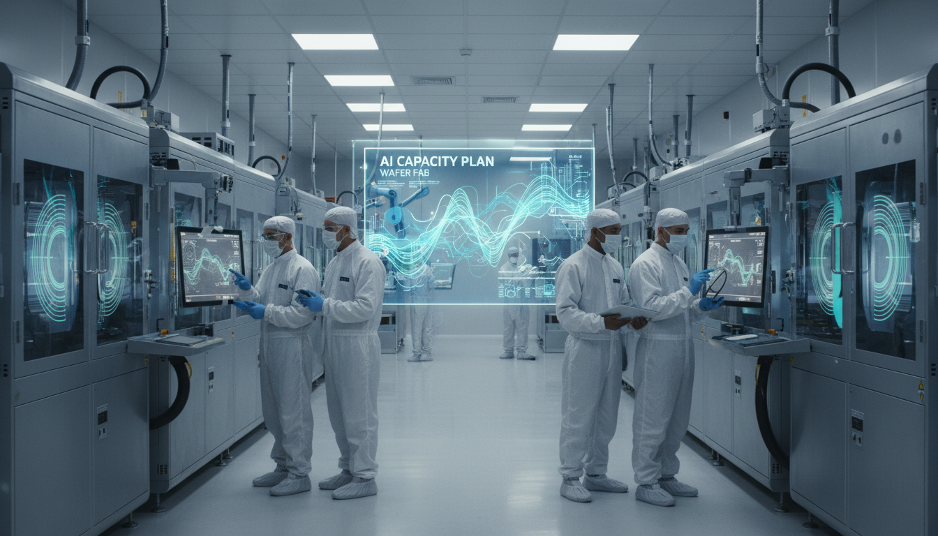
AI Capacity Plan Wafer Fab
The concept of " AI Capacity Plan Wafer Fab" refers to the integration of artificial intelligence into the operational frameworks of wafer fabrication facilities , particularly within the Silicon Wafer Engineering sector. This approach emphasizes optimizing production processes, enhancing quality control, and streamlining resource allocation. As stakeholders navigate an increasingly complex landscape, this strategic alignment with AI-led transformation becomes essential for maintaining competitiveness and addressing rising operational demands.
In the Silicon Wafer Engineering ecosystem, the AI Capacity Plan Wafer Fab is pivotal for redefining competitive dynamics and fostering innovation. AI-driven methodologies are reshaping how stakeholders interact, influencing everything from decision-making to collaboration. The adoption of these advanced practices not only enhances efficiency but also guides long-term strategic direction. However, the journey towards full integration presents challenges, including adoption barriers and the complexity of aligning new technologies with existing operations, which must be addressed to unlock the potential for growth and transformation.
Accelerate AI Adoption in Wafer Fab Operations
Silicon Wafer Engineering companies should strategically invest in AI Capacity Plan Wafer Fab initiatives and forge partnerships with leading AI technology firms to enhance process automation and data analytics. By embracing AI, companies can achieve significant operational efficiencies, reduce production costs, and gain a competitive edge in the rapidly evolving semiconductor market.
How AI is Transforming Wafer Fab Capacity Planning?
Implementation Framework
Evaluate current capabilities and gaps
Deploy AI technologies in processes
Track AI system effectiveness
Enhance logistics through AI
Develop skills for AI adoption
Conduct a thorough assessment of existing capabilities and identify gaps in AI readiness . This ensures that the AI Capacity Plan aligns with operational goals, enhancing productivity and innovation in wafer fabrication .
Internal R&D
Implement AI-driven solutions within wafer fabrication processes to automate tasks and optimize production. This integration can significantly reduce waste and improve yield, driving competitive advantages in the market.
Technology Partners
Establish key performance indicators (KPIs) to evaluate AI systems' performance in wafer production . Regular monitoring allows for adjustments that enhance operational efficiency and support continuous improvement strategies across the facility.
Industry Standards
Utilize AI analytics to optimize supply chain logistics, predicting demand and improving inventory management. This optimization reduces lead times and enhances responsiveness, ultimately increasing customer satisfaction and operational resilience.
Cloud Platform
Implement training programs focused on AI technologies to equip employees with necessary skills. A skilled workforce enhances AI integration, promotes innovation, and strengthens the company's competitive position in the wafer fabrication market.
Internal R&D
Best Practices for Automotive Manufacturers
Integrate AI Algorithms Effectively
- Impact : Enhances defect detection accuracy significantly
Example : Example: In a silicon wafer fab , AI algorithms analyze defect patterns in real-time, achieving 95% accuracy in detecting anomalies, leading to a significant reduction in total rework hours across production lines. - Impact : Reduces production downtime and costs
Example : Example: A wafer fabrication facility implements AI to predict machine failures. This proactive approach reduces unplanned downtime by 40%, saving the company thousands in daily operational costs. - Impact : Improves quality control standards
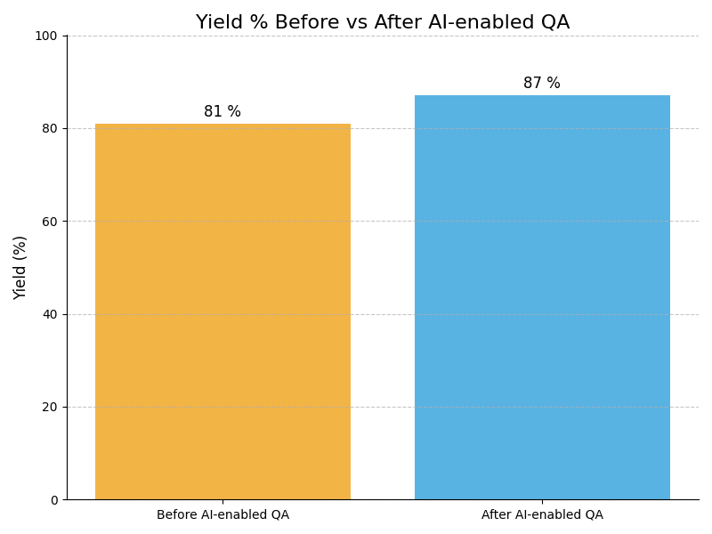
Example : Example: An AI-based quality assurance system monitors wafer characteristics continuously, catching defects before they escalate, thus improving quality control metrics by 30% and enhancing customer satisfaction. - Impact : Boosts overall operational efficiency
Example : Example: By utilizing AI for process optimization, a fab increases throughput by 20%, allowing for more wafers to be produced in peak times without compromising quality.
- Impact : High initial investment for implementation
Example : Example: A major semiconductor manufacturer postpones its AI deployment due to the high costs of new hardware and software, delaying anticipated efficiency gains and market competitiveness. - Impact : Potential data privacy concerns
Example : Example: During AI integration, sensitive production data is mishandled, raising alarms about compliance with data protection regulations, and causing internal audits that slow down the project. - Impact : Integration challenges with existing systems
Example : Example: An AI system fails to integrate with legacy equipment, forcing engineers to revert to manual data collection methods, thereby undermining the automation goals and increasing labor costs. - Impact : Dependence on continuous data quality
Example : Example: Inconsistent sensor data leads to inaccurate AI predictions about wafer quality, causing a spike in production errors and resulting in increased waste and rework costs.
Utilize Real-time Monitoring
- Impact : Improves process control and stability
Example : Example: In a wafer fabrication facility, real-time monitoring systems track equipment performance, leading to a 25% increase in operational stability and allowing for timely adjustments before any significant issues arise. - Impact : Enhances predictive maintenance capabilities
Example : Example: A semiconductor plant implements AI-driven predictive maintenance, which identifies wear patterns in machinery, reducing unexpected failures by 35% and optimizing maintenance schedules. - Impact : Reduces manual oversight requirements
Example : Example: Utilizing real-time monitoring reduces the need for manual checks by 50%, freeing up engineers to focus on higher-level tasks, ultimately improving team productivity. - Impact : Facilitates quicker decision-making processes
Example : Example: AI-enabled dashboards provide real-time insights, allowing managers to make informed decisions quickly, reducing response time to production issues by 40%.
- Impact : Dependence on technology reliability
Example : Example: A silicon wafer manufacturer encounters downtime when their real-time monitoring system fails, highlighting the dependency on technology and emphasizing the need for robust backup plans to prevent losses. - Impact : High costs of integration and updates
Example : Example: Upgrading a monitoring system incurs significant costs, causing budget overruns and delaying other critical projects that could improve production efficiency. - Impact : Potential for data overload
Example : Example: An influx of data from real-time monitoring overwhelms the analysis team, leading to critical insights being missed and decision-making paralysis during production peaks. - Impact : Requires skilled personnel for management
Example : Example: A fab struggles to find qualified personnel to manage and interpret data from monitoring systems, causing delays in optimizing production processes and hampering overall effectiveness.
Train Workforce Regularly
- Impact : Enhances employee skill sets and knowledge
Example : Example: A silicon wafer fab implements regular training programs, resulting in a 30% increase in employee proficiency with AI tools, thereby reducing operational errors and boosting overall productivity. - Impact : Increases adaptability to new technologies
Example : Example: By training employees on the latest AI technologies, a semiconductor manufacturer increases adaptability, allowing teams to implement new systems 20% faster than before, streamlining operations significantly. - Impact : Reduces operational errors and inefficiencies
Example : Example: Comprehensive training reduces errors in wafer processing , leading to a 15% decrease in waste, which is crucial for maintaining profitability in a competitive market. - Impact : Promotes a culture of continuous improvement
Example : Example: Fostering a culture of continuous improvement through regular training initiatives helps a fab adapt quickly to market changes, enhancing its responsiveness and overall competitiveness.
- Impact : Potential resistance to change
Example : Example: A semiconductor company faces pushback from veteran employees hesitant to adapt to AI tools, which hampers implementation and slows down overall productivity improvements in the factory. - Impact : Training costs may exceed budget
Example : Example: The cost of extensive training programs surpasses initial budget estimates, forcing management to reallocate funds from other vital projects, impacting overall efficiency. - Impact : Varied learning paces among employees
Example : Example: The diverse learning speeds among employees lead to uneven adoption of AI tools, resulting in inconsistent performance across teams and creating inefficiencies in production processes. - Impact : Difficulty measuring training effectiveness
Example : Example: Measuring the effectiveness of training programs proves challenging, leaving management uncertain about the return on investment and hindering future training decisions.
Adopt Agile Methodologies
- Impact : Boosts innovation and responsiveness
Example : Example: A silicon wafer fab adopts agile methodologies, enabling faster iterations in process development, leading to a 25% reduction in time-to-market for new products, enhancing competitiveness. - Impact : Facilitates effective cross-functional collaboration
Example : Example: Cross-functional teams in a semiconductor plant using agile practices report improved collaboration, resulting in 30% faster problem resolution and a more cohesive working environment. - Impact : Shortens development cycles significantly
Example : Example: Iterative feedback loops in product development improve overall quality, with defect rates dropping by 20% as teams swiftly address issues during the production process. - Impact : Enhances product quality through iterative feedback
Example : Example: An agile approach shortens development cycles, allowing a fab to launch new tech solutions in response to market demands, securing a stronger position in the industry.
- Impact : Requires cultural shift in organization
Example : Example: A semiconductor manufacturer struggles with resistance during the cultural shift towards agile methodologies, slowing down the adoption process and limiting innovation opportunities. - Impact : Team dynamics can become challenging
Example : Example: A newly formed agile team experiences friction as members adjust to collaborative workflows, causing delays in project timelines and affecting overall productivity in the fab. - Impact : Initial implementation may face resistance
Example : Example: Initial implementation of agile practices faces pushback from traditional managers, leading to a fragmented approach that hinders project momentum and team morale. - Impact : May lead to scope creep in projects
Example : Example: A project team faces scope creep as agile practices lead to frequent changes in project requirements, resulting in resource allocation challenges and potential delays in deliverables.
Implement AI-driven Process Optimization
- Impact : Maximizes resource utilization and efficiency
Example : Example: A silicon wafer fab implements AI-driven optimization techniques, resulting in a 40% increase in resource utilization, allowing for better management of raw materials across processes. - Impact : Decreases cycle times significantly
Example : Example: AI algorithms analyze production workflows, decreasing cycle times by 30%, enabling the fab to produce more wafers within the same time frame and improve overall output. - Impact : Enhances throughput and yield rates
Example : Example: By employing AI for process optimization, a semiconductor plant sees yield rates improve by 25%, directly impacting profitability and market share in a competitive landscape. - Impact : Improves overall production consistency
Example : Example: AI-driven adjustments to production parameters enhance consistency across batches, reducing variability and ensuring higher quality standards are consistently met.
- Impact : Complexity of system integration
Example : Example: A fab faces significant challenges during the integration of new AI systems with existing machinery, causing delays in production ramp-up and resulting in financial losses due to inefficiencies. - Impact : Requires ongoing maintenance and updates
Example : Example: The ongoing maintenance required for AI-driven systems strains resources, as engineers are needed to troubleshoot and update algorithms, diverting attention from core production tasks. - Impact : Potential for AI biases in decisions
Example : Example: An AI system misinterprets data due to inherent biases, leading to faulty process adjustments that compromise product quality and increase scrap rates in the fab. - Impact : Over-reliance on automated processes
Example : Example: Over-reliance on AI automation leads to a lack of manual oversight, resulting in unnoticed errors that escalate into larger production issues, ultimately affecting output quality.
Enhance Data Management Practices
- Impact : Improves data accuracy and reliability
Example : Example: A silicon wafer manufacturing facility enhances its data management processes, leading to a 50% increase in data accuracy, which is crucial for maintaining high production standards and reducing errors. - Impact : Facilitates better decision-making
Example : Example: Improved data management allows for informed decision-making in a semiconductor plant, resulting in a 20% increase in operational efficiency and timely adjustments to production lines. - Impact : Enables real-time analytics capabilities
Example : Example: By enabling real-time analytics through better data practices, a fab reduces response times to production issues by 35%, significantly improving overall workflow and productivity. - Impact : Supports compliance with industry standards
Example : Example: A fab's enhanced data management ensures compliance with strict industry standards, preventing potential fines and maintaining credibility in the competitive semiconductor market.
- Impact : Data security and breach risks
Example : Example: A semiconductor manufacturer faces a significant data breach due to inadequate security measures in their data management system, leading to lost trust and expensive remediation efforts. - Impact : High costs of data management systems
Example : Example: The high costs associated with implementing advanced data management systems exceed budget forecasts, forcing the company to delay other critical operational upgrades. - Impact : Integration with legacy systems may falter
Example : Example: Integration efforts between new data management systems and outdated legacy software fail, resulting in data silos that hamper communication and decision-making across departments. - Impact : Reliance on accurate data source availability
Example : Example: A fab struggles with data availability as system outages occur, leading to delays in real-time decision-making and negatively impacting production timelines.
We manufactured the most advanced AI chips in the world, in the most advanced fab in the world, here in America for the first time, marking the beginning of expanded AI capacity planning in US wafer fabs.
– Jensen Huang, CEO of NvidiaCompliance Case Studies

_case_study.png)

Seize the opportunity to leverage AI-driven solutions for your capacity planning. Transform challenges into competitive advantages and elevate your Silicon Wafer Engineering processes today!
Take Test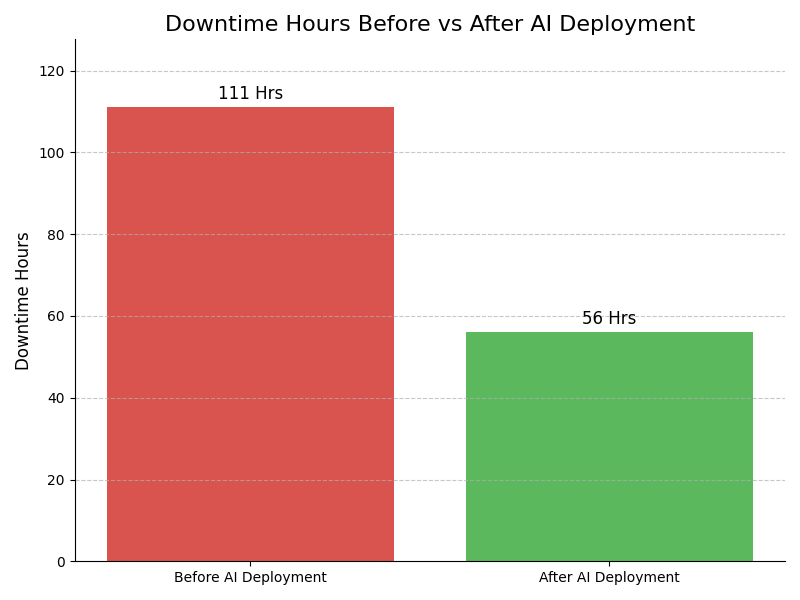
Leadership Challenges & Opportunities
Data Integration Challenges
Utilize AI Capacity Plan Wafer Fab to create a unified data ecosystem by integrating disparate data sources through advanced APIs. This technology enhances data visibility and quality, enabling real-time analytics and decision-making, which optimizes wafer fabrication processes and improves overall efficiency.
Cultural Resistance to Change
Implement change management strategies alongside AI Capacity Plan Wafer Fab to foster a culture of innovation. Engage stakeholders with workshops and demonstrations showcasing AI benefits, ensuring buy-in and reducing resistance. This promotes a proactive approach to adopting new technologies and enhances team collaboration.
High Operational Costs
Adopt AI Capacity Plan Wafer Fab using predictive analytics to forecast demand and optimize resource allocation, thus reducing waste. Implementing cost-efficient AI-driven solutions can streamline operations, leading to significant savings and improved profit margins in wafer fabrication processes.
Regulatory Compliance Complexity
AI Capacity Plan Wafer Fab offers automated compliance management features that simplify adherence to industry regulations. By integrating real-time monitoring and reporting tools, companies can quickly adapt to regulatory changes, ensuring ongoing compliance and minimizing risks associated with audits and penalties.
Assess how well your AI initiatives align with your business goals
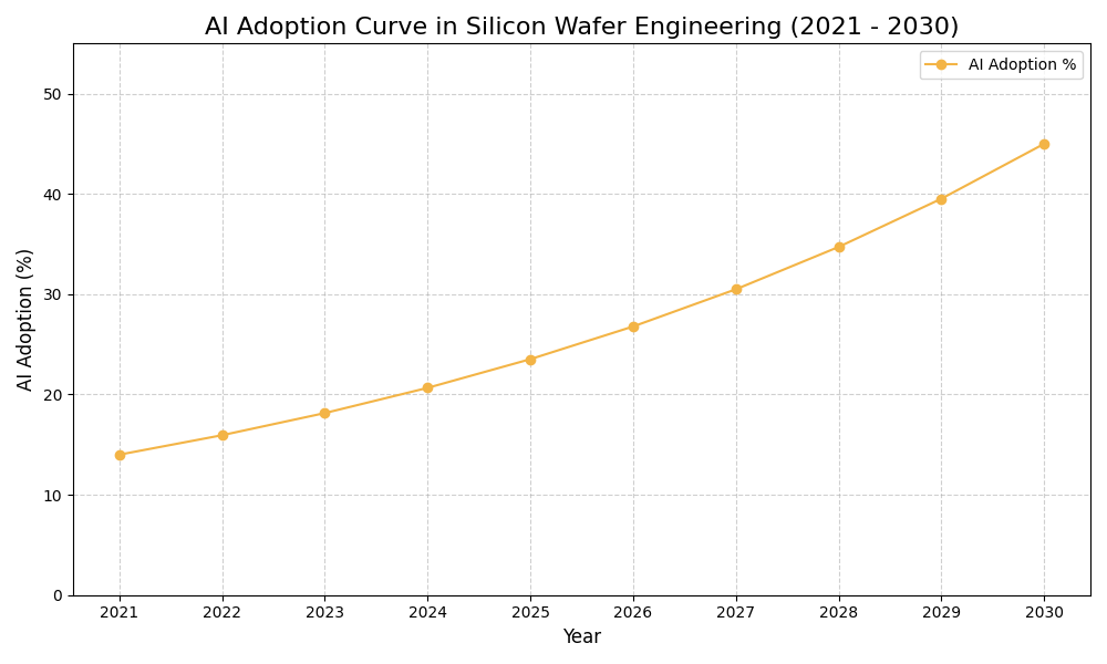
AI Adoption Graph
AI Use Case vs ROI Timeline
| AI Use Case | Description | Typical ROI Timeline | Expected ROI Impact |
|---|---|---|---|
| Predictive Maintenance for Equipment | AI can monitor equipment health in real-time, predicting failures before they happen. For example, sensors analyze temperature and vibration data to forecast maintenance needs, reducing downtime significantly in wafer fabrication processes. | 6-12 months | High |
| Yield Optimization through AI Analytics | Implementing AI analytics can identify factors affecting yield rates. For example, AI algorithms analyze historical production data to optimize parameters, resulting in enhanced wafer yield and reduced scrap rates in manufacturing. | 12-18 months | Medium-High |
| Supply Chain Demand Forecasting | AI can enhance supply chain efficiency by predicting material demand accurately. For example, machine learning models analyze past usage patterns to ensure timely procurement of silicon wafers, minimizing delays. | 6-12 months | Medium |
| Automated Quality Control Systems | AI-driven vision systems can inspect silicon wafers for defects in real-time. For example, computer vision algorithms detect anomalies during production, ensuring only high-quality wafers proceed to the next stage. | 6-12 months | High |
Glossary
Work with Atomic Loops to architect your AI implementation roadmap — from PoC to enterprise scale.
Contact NowFrequently Asked Questions
- Begin by assessing your current wafer fab processes to identify improvement areas.
- Engage stakeholders to align on objectives and expected outcomes for AI integration.
- Invest in training programs to ensure staff are equipped with necessary AI skills.
- Select a pilot project to test AI tools before full-scale implementation.
- Establish clear metrics to evaluate the pilot's success and scalability.
- AI integration can significantly improve production efficiency and yield rates.
- It enables predictive maintenance, reducing downtime and operational costs.
- Firms can achieve faster decision-making through real-time data analytics.
- Enhanced quality control leads to fewer defects and higher customer satisfaction.
- Companies gain competitive advantages through innovation and faster time-to-market.
- Resistance to change from staff may hinder smooth AI adoption and integration.
- Data quality issues can impact the effectiveness of AI algorithms significantly.
- Integration with legacy systems can pose technical hurdles during implementation.
- Skill gaps in the workforce may necessitate extensive training and support.
- Unforeseen costs may arise, requiring careful budgeting and resource allocation.
- Organizations should adopt AI when they have sufficient data to train models effectively.
- Timing aligns well with digital transformation initiatives or process overhauls.
- Evaluate industry trends and competitor strategies to gauge market readiness.
- Consider internal capacity and resources before initiating an AI project.
- Launching during periods of low production may reduce operational disruption.
- AI can optimize the supply chain, improving material flow and inventory management.
- It enhances equipment monitoring, predicting failures before they occur.
- AI algorithms can refine process parameters for better yield and lower costs.
- Customer demand forecasting can be improved through AI-driven analytics.
- Regulatory compliance can be streamlined using AI for better reporting and audits.
- Establish baseline metrics before AI adoption to compare post-implementation results.
- Track changes in production efficiency and defect rates over time.
- Analyze cost savings achieved from reduced downtime and maintenance needs.
- Evaluate improvements in customer satisfaction and retention metrics.
- Regularly review metrics to ensure alignment with business goals and objectives.
- Conduct thorough risk assessments during the planning phase to identify potential challenges.
- Implement a phased rollout to minimize disruption and allow for adjustments.
- Engage in continuous monitoring and feedback loops to refine AI applications.
- Develop contingency plans for unexpected failures or bottlenecks during implementation.
- Foster a culture of adaptability and resilience within the organization to navigate changes.
- Start with clear goals and objectives to guide AI project development effectively.
- Involve cross-functional teams to leverage diverse expertise and perspectives.
- Prioritize data quality and governance to enhance AI model performance.
- Establish a robust change management framework to ease staff transitions.
- Continuously evaluate and iterate on AI strategies for long-term success.