AI Bottleneck Wafer Fab Finder
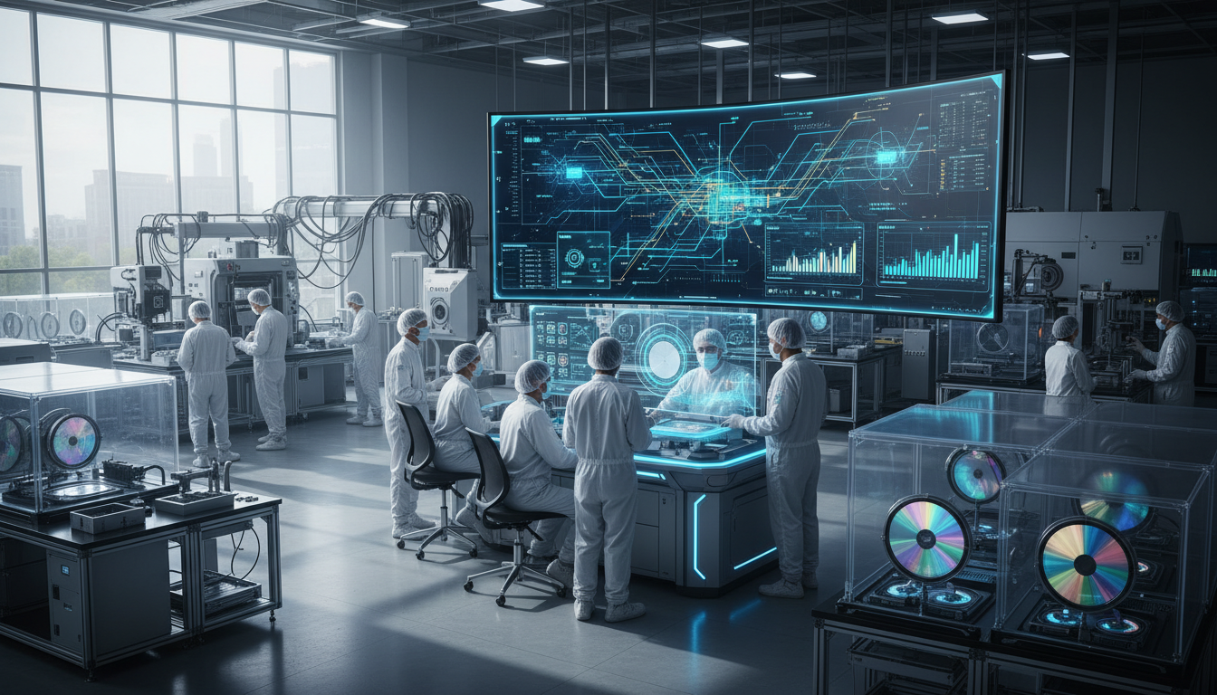
In the realm of Silicon Wafer Engineering, the " AI Bottleneck Wafer Fab Finder" represents a pivotal advancement that leverages artificial intelligence to identify and mitigate production bottlenecks within semiconductor fabrication. This concept encapsulates the integration of intelligent algorithms into manufacturing processes, enhancing operational efficiency and responsiveness. As the industry grapples with increasing complexity and demand for high-performance chips, the relevance of this innovation resonates deeply with stakeholders seeking to optimize their supply chains and production workflows. It embodies the broader trend of AI-led transformation, positioning organizations to better align with evolving strategic priorities and technological advancements.
The Silicon Wafer Engineering ecosystem is undergoing a significant metamorphosis driven by AI-powered innovations like the Bottleneck Wafer Fab Finder. These advancements not only redefine competitive dynamics but also accelerate innovation cycles and enhance collaboration among stakeholders. By adopting AI practices, organizations are witnessing improvements in operational efficiency, informed decision-making, and strategic agility . However, the path to widespread AI integration is fraught with challenges, including adoption hurdles and complexities in implementation. As organizations navigate these realities, the potential for growth remains robust, underscoring a landscape ripe with opportunities for those willing to adapt.
Maximize Efficiency with AI-Powered Wafer Production Strategies
Silicon Wafer Engineering companies should strategically invest in partnerships focused on AI-driven solutions to optimize the bottleneck wafer fabrication process. Implementing these AI technologies is expected to enhance production efficiency, reduce costs, and provide a significant competitive edge in the market.
How AI is Transforming the Silicon Wafer Engineering Landscape?
Implementation Framework
Evaluate current capabilities for AI implementation
Develop a robust data management framework
Adopt AI solutions for efficiency gains
Upskill employees on AI technologies
Continuously evaluate AI impact and performance
Conduct a thorough assessment of existing AI capabilities within the organization to identify gaps. This evaluation is essential for determining the necessary resources and skills to effectively adopt AI technologies in wafer fabrication .
Internal R&D
Create a comprehensive data strategy that encompasses data collection, storage, and processing. A well-defined strategy is critical for ensuring the availability of high-quality data essential for AI-driven insights in wafer fabrication .
Technology Partners
Integrate advanced AI tools and algorithms into existing fabrication processes to enhance efficiency and reduce bottlenecks. This integration is crucial for operational optimization and maximizing production capacity in silicon wafer engineering .
Industry Standards
Implement training programs for employees to enhance their understanding and skills in AI technologies. A well-trained workforce is essential for successful AI implementation, ensuring that staff can effectively utilize new tools and practices.
Internal R&D
Establish a framework for monitoring the performance of AI systems and their impact on fabrication processes. Regular evaluations are vital for identifying areas of improvement and ensuring that AI applications continue to deliver value in silicon wafer engineering operations.
Cloud Platform
Best Practices for Automotive Manufacturers
Optimize Data Flow Efficiently
- Impact : Increases data processing speed significantly
Example : Example: A silicon wafer fab optimized its data flow by integrating edge computing, resulting in a 30% increase in processing speed, enabling engineers to make faster decisions on production adjustments. - Impact : Enhances real-time decision-making capabilities
Example : Example: By using real-time data analytics, a wafer fab reduced the time needed for quality control decisions by 40%, allowing for quicker adjustments and improved yield rates during high-demand periods. - Impact : Improves overall system responsiveness
Example : Example: An AI system analyzes data streams from sensors continuously, providing engineers with actionable insights that improve system responsiveness by 25%, leading to optimized production cycles. - Impact : Facilitates better resource allocation
Example : Example: Effective data flow management allowed a fab to allocate resources dynamically, reducing machine idle time by 20% during peak hours, maximizing output without increasing costs.
- Impact : Complexity in managing large data sets
Example : Example: A wafer fab faced significant delays in production when it struggled to manage the influx of data from new AI systems, resulting in a backlog that hindered operational efficiency. - Impact : Increased vulnerability to cyber threats
Example : Example: Following a cyberattack, a semiconductor manufacturer discovered vulnerabilities in their AI data handling processes, leading to compromised production data and costly downtime. - Impact : Challenges with data integration
Example : Example: Integration issues arose when an AI tool was unable to work seamlessly with existing data sources, causing delays in critical decision-making processes and impacting production schedules. - Impact : Need for ongoing system maintenance
Example : Example: A reliance on AI systems for data processing led to several unplanned maintenance outages, as outdated hardware could not keep pace, disrupting production and impacting overall efficiency.
Integrate AI Algorithms Effectively
- Impact : Enhances defect detection accuracy significantly
Example : Example: In a silicon wafer production line, an AI algorithm detects microscopic surface defects in real-time, reducing rejection rates by 15% and minimizing costly rework by identifying issues during production. - Impact : Reduces production downtime and costs
Example : Example: A semiconductor manufacturer implemented AI to analyze machine performance, leading to a 20% reduction in downtime by predicting failures before they occurred, significantly saving costs. - Impact : Improves quality control standards
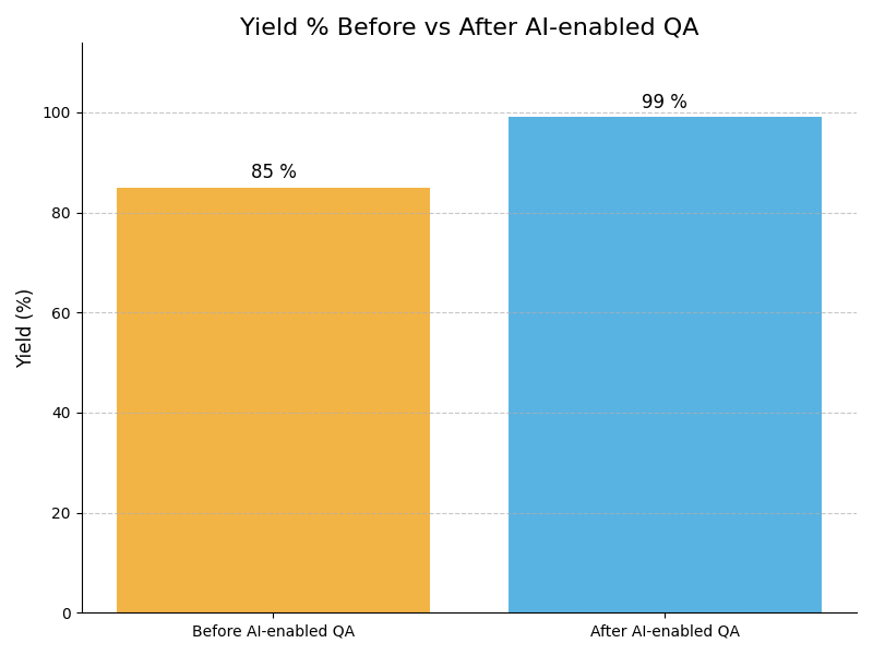
Example : Example: AI algorithms monitor production quality continuously, leading to a 30% improvement in compliance with quality control standards, as defects are identified and addressed immediately. - Impact : Boosts overall operational efficiency
Example : Example: By optimizing operational workflows with AI, a wafer fab saw a 25% boost in overall efficiency, enabling them to meet rising demand without additional resources.
- Impact : High initial investment for implementation
Example : Example: A mid-sized electronics manufacturer delayed the AI rollout after realizing that the cost of new camera hardware and GPUs exceeded their budget, pushing back implementation timelines significantly. - Impact : Potential data privacy concerns
Example : Example: The AI system's data capture inadvertently stored sensitive operational data, raising compliance concerns and forcing the company to review its data governance protocols. - Impact : Integration challenges with existing systems
Example : Example: Integration with legacy systems proved problematic, as AI tools struggled to communicate with outdated equipment, leading to manual processes that slowed production. - Impact : Dependence on continuous data quality
Example : Example: The AI's reliance on high-quality data became evident when incorrect data inputs led to erroneous defect classifications, resulting in a production halt and loss of revenue.
Train Workforce Regularly
- Impact : Enhances team technical skillsets
Example : Example: A silicon wafer fab implemented a regular training program on AI tools, resulting in a 40% increase in technical skill levels among staff, empowering them to leverage new technologies effectively. - Impact : Promotes a culture of innovation
Example : Example: By fostering a culture of continuous learning, a manufacturer saw a 30% rise in innovative project proposals from staff, as employees felt more equipped to contribute with their new skills. - Impact : Reduces resistance to AI adoption
Example : Example: Regular training sessions reduced resistance to AI adoption by 50%, as employees became more familiar with the technology and its benefits, leading to smoother transitions in workflows. - Impact : Improves collaboration across teams
Example : Example: Enhanced collaboration across teams was observed when employees from different departments participated in joint training, improving communication and project execution by 25%.
- Impact : Inconsistent training across departments
Example : Example: A wafer fab faced inconsistent AI training across departments, leading to varying levels of competency and confusion during cross-functional projects, ultimately delaying important initiatives. - Impact : Potential skill gaps among employees
Example : Example: Skill gaps became apparent when teams unable to effectively use AI tools struggled with decision-making, causing delays in production adjustments and losses in efficiency. - Impact : Resistance to change from staff
Example : Example: Employees resisted AI changes due to a lack of understanding of the technology's benefits, leading to friction within teams and slowing down implementation timelines significantly. - Impact : Ongoing training costs may escalate
Example : Example: As training programs expanded, ongoing costs escalated beyond initial projections, straining the budget and leading management to reassess the training strategy.
Utilize Real-time Monitoring
- Impact : Improves operational visibility significantly
Example : Example: A silicon wafer fab implemented real-time monitoring systems on critical machinery, improving operational visibility by 50% and enabling quicker responses to potential issues. - Impact : Facilitates immediate response to issues
Example : Example: With real-time data on machine performance, a semiconductor manufacturer reduced equipment failure rates by 30%, minimizing production interruptions and enhancing throughput. - Impact : Reduces equipment failure rates
Example : Example: AI predictive maintenance tools analyze operational data in real-time, allowing a fab to preemptively address maintenance needs, reducing downtime by 25% and optimizing resource use. - Impact : Enhances predictive maintenance capabilities
Example : Example: Real-time monitoring enabled a wafer fab to identify and rectify quality issues immediately, leading to a 40% reduction in defective products and enhancing overall production quality.
- Impact : Costs associated with monitoring technology
Example : Example: The implementation of advanced monitoring technology at a semiconductor plant resulted in high upfront costs, leading management to reconsider the budget allocations for production enhancements. - Impact : Potential overload of data for analysis
Example : Example: A fab experienced data overload, as the volume of real-time information generated became overwhelming, complicating analysis and delaying decision-making processes. - Impact : Integration with existing systems can be complex
Example : Example: Integration of new monitoring systems with legacy equipment proved complex, resulting in unexpected delays in implementation and disrupting production schedules. - Impact : Requires skilled personnel for oversight
Example : Example: The need for skilled personnel to oversee monitoring systems became apparent when existing staff struggled to interpret data, causing delays in critical operational decisions.
Leverage AI for Predictive Analytics
- Impact : Enhances forecasting accuracy significantly
Example : Example: A silicon wafer manufacturer leveraged AI for predictive analytics, improving forecasting accuracy by 35%, allowing for better alignment of production schedules with market demand. - Impact : Improves resource management efficiency
Example : Example: By utilizing AI-driven analytics, a fab enhanced resource management efficiency by 25%, optimizing material usage and reducing waste during production. - Impact : Reduces operational costs substantially
Example : Example: Predictive analytics reduced operational costs by 20% at a semiconductor plant by identifying inefficiencies and enabling targeted improvements in workflows. - Impact : Facilitates faster decision-making processes
Example : Example: AI tools facilitated faster decision-making processes, enabling a wafer fab to respond to market changes swiftly, thereby increasing competitiveness and customer satisfaction.
- Impact : Dependence on accurate historical data
Example : Example: A silicon wafer fab faced challenges when its predictive analytics models failed due to inaccuracies in historical data, leading to misguided production forecasts and excess inventory. - Impact : Complexity in model development
Example : Example: The complexity of developing predictive models caused significant delays in implementation, frustrating teams eager to leverage AI capabilities in their operations. - Impact : Resistance to reliance on AI
Example : Example: Employees resisted relying on AI for decision-making, leading to a lack of trust in analytics results, which hampered the integration of AI into standard operational practices. - Impact : Potential misinterpretation of analytics results
Example : Example: Misinterpretation of predictive analytics led to erroneous decisions at a semiconductor plant, causing disruptions in production and impacting overall efficiency.
Implement Continuous Improvement Practices
- Impact : Fosters a culture of innovation
Example : Example: A silicon wafer fab adopted continuous improvement practices, fostering a culture of innovation that led to a 30% increase in process enhancements over two years, significantly boosting output. - Impact : Enhances adaptability to changes
Example : Example: By implementing regular reviews, a semiconductor manufacturer improved adaptability to market changes, enabling a 25% quicker response to new technology trends and customer demands. - Impact : Improves long-term sustainability
Example : Example: Continuous improvement initiatives enhanced sustainability efforts, reducing energy consumption by 15% in a wafer fab while maintaining production levels, contributing to environmental goals. - Impact : Drives operational excellence consistently
Example : Example: The focus on operational excellence drove consistent performance improvements, resulting in a 20% increase in overall efficiency and better alignment with strategic objectives.
- Impact : Resistance to continuous change
Example : Example: A silicon wafer fab encountered resistance to continuous change initiatives, as employees were hesitant to alter established workflows, stalling progress in operational enhancements. - Impact : Difficulty in measuring improvements
Example : Example: Difficulty in measuring improvements led to confusion over the effectiveness of continuous improvement practices, causing frustration among teams eager to see tangible results. - Impact : Potential over-reliance on past successes
Example : Example: A reliance on past successes hindered innovation, as teams became complacent, failing to explore new methods that could have further enhanced production efficiency. - Impact : Need for ongoing leadership commitment
Example : Example: Continuous improvement efforts faltered due to a lack of ongoing leadership commitment, resulting in diminished employee morale and a decline in initiative participation.
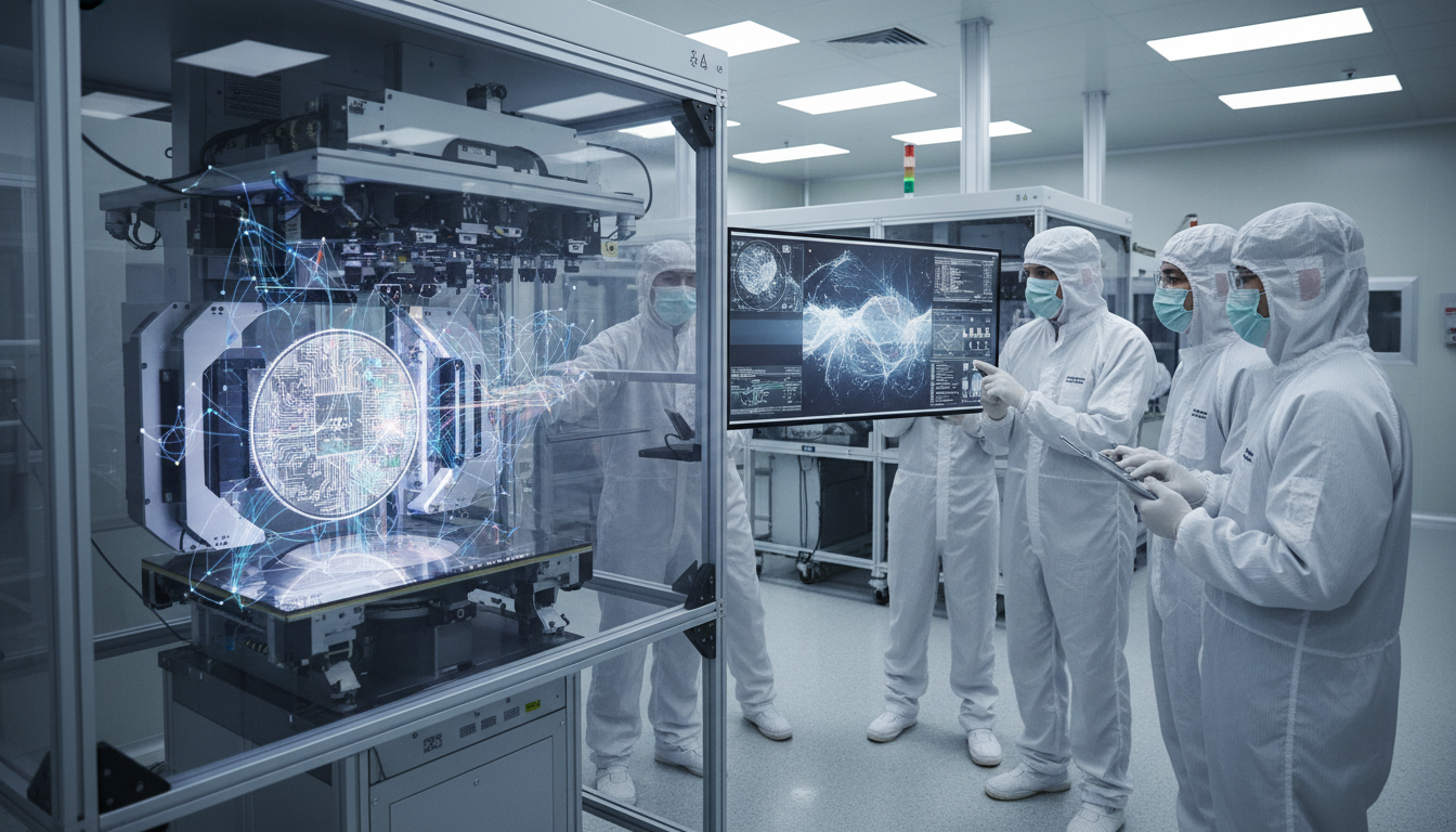
AI and machine learning are playing an integral role in helping us achieve quality, efficiency, and competitiveness across various stages of wafer production by addressing equipment bottlenecks through predictive maintenance and anomaly detection.
– WaferPro Team, Director of Manufacturing Operations, WaferProCompliance Case Studies

Embrace AI now to eliminate bottlenecks in wafer fabrication . Transform your operations and secure a competitive edge in Silicon Wafer Engineering .
Take Test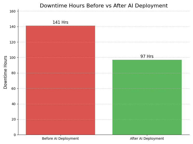
Leadership Challenges & Opportunities
Data Integration Challenges
Utilize AI Bottleneck Wafer Fab Finder's advanced algorithms to harmonize disparate data sources across Silicon Wafer Engineering. By implementing automated data pipelines and real-time analytics, organizations can achieve seamless integration, enhancing decision-making and operational efficiency.
Change Management Resistance
Facilitate a smooth transition to AI Bottleneck Wafer Fab Finder by fostering an inclusive culture. Engage stakeholders through workshops and demonstrations, highlighting the technology's benefits. Implement feedback loops to address concerns and encourage adoption, ensuring alignment with organizational goals.
High Operational Costs
Employ AI Bottleneck Wafer Fab Finder to optimize resource allocation and operational workflows. Use predictive analytics to identify inefficiencies and reduce waste, leading to cost savings. Implement a phased rollout focused on high-impact areas to demonstrate value and secure further investment.
Compliance with Industry Standards
Integrate AI Bottleneck Wafer Fab Finder with regulatory frameworks to ensure compliance in Silicon Wafer Engineering. Utilize its compliance monitoring features to automate reporting and audit processes, helping organizations stay ahead of regulations while minimizing risks and improving transparency.
Assess how well your AI initiatives align with your business goals
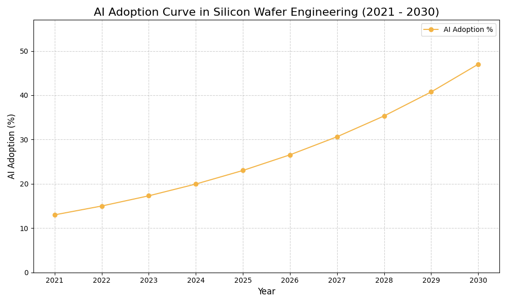
AI Adoption Graph
AI Use Case vs ROI Timeline
| AI Use Case | Description | Typical ROI Timeline | Expected ROI Impact |
|---|---|---|---|
| Predictive Maintenance for Equipment | AI algorithms analyze equipment data to predict failures before they occur, minimizing downtime. For example, predictive models can alert technicians about potential breakdowns in photolithography machines, ensuring timely maintenance and avoiding costly production halts. | 6-12 months | High |
| Yield Optimization through AI Analytics | Utilizing AI to analyze production data helps identify factors affecting yield rates. For example, AI can optimize chemical processes in etching to increase yield rates by 15%, reducing material waste and enhancing profitability. | 12-18 months | Medium-High |
| Supply Chain Demand Forecasting | AI-driven forecasting tools improve supply chain management by predicting demand fluctuations. For example, using historical sales data, AI can optimize raw material orders for silicon wafers, reducing excess inventory costs. | 6-9 months | Medium |
| Automated Defect Detection | AI systems enhance quality control by automatically detecting defects in wafers during production. For example, computer vision systems can identify microscopic defects in real-time, allowing for immediate corrective actions and reducing rejection rates. | 9-12 months | High |
Glossary
Work with Atomic Loops to architect your AI implementation roadmap — from PoC to enterprise scale.
Contact NowFrequently Asked Questions
- AI Bottleneck Wafer Fab Finder identifies process inefficiencies in wafer fabrication.
- It employs machine learning to analyze production data and highlight bottlenecks.
- This tool enhances throughput by optimizing workflow and resource allocation.
- Companies benefit from reduced cycle times and improved yield rates.
- It ultimately leads to more efficient operations and better cost management.
- Begin by assessing current manufacturing workflows and identifying pain points.
- Involve cross-functional teams to ensure comprehensive understanding of processes.
- Develop a pilot project to test AI solutions on a smaller scale first.
- Allocate resources and establish a timeline for full implementation.
- Regularly review progress and adjust strategies based on initial findings.
- AI solutions can lead to significant reductions in operational costs and waste.
- Companies frequently report improved production efficiency and cycle times.
- Enhanced data analytics help in making informed strategic decisions.
- Organizations can achieve higher yield rates and better product quality.
- These improvements translate into a stronger competitive edge in the market.
- Resistance to change from employees can hinder adoption of AI technologies.
- Data quality issues can affect the accuracy of AI-driven insights.
- Integration with legacy systems may pose technical difficulties during implementation.
- Training staff to effectively use AI tools is essential for success.
- Establishing clear goals and metrics can help overcome these challenges.
- Organizations should consider adopting AI when facing consistent production delays.
- If existing processes yield diminishing returns, AI can provide necessary improvements.
- Market competition may necessitate quicker innovation cycles and efficiencies.
- Timing is critical; early adoption can position companies as industry leaders.
- Regularly assess operational performance to identify optimal adoption opportunities.
- AI can optimize yield analysis by identifying and mitigating process variabilities.
- Predictive maintenance reduces downtime by anticipating equipment failures.
- Process optimization ensures that fabrication meets strict industry standards.
- Real-time monitoring can enhance quality control throughout the manufacturing process.
- These applications contribute to overall operational excellence and compliance.
- Establish clear KPIs to track performance before and after implementation.
- Measure reductions in cycle times and overall production efficiency gains.
- Analyze cost savings from reduced waste and improved resource utilization.
- Collect feedback from teams to evaluate qualitative benefits such as morale.
- Regularly review financial metrics to ensure sustained return on investment.
- Ensure compliance with industry standards and regulations related to data security.
- Understand the implications of AI decision-making on product quality and safety.
- Regular audits can help maintain adherence to compliance requirements.
- Engage legal counsel to navigate complex regulatory landscapes effectively.
- Staying informed about evolving regulations is crucial for ongoing compliance.