
AI Adoption Fab Case Studies
In the realm of Silicon Wafer Engineering, "AI Adoption Fab Case Studies" represents a pivotal exploration of how artificial intelligence is integrated into fabrication processes. This concept encompasses a variety of practical scenarios where AI technologies enhance operational efficiencies and decision-making frameworks. As the industry embraces AI, stakeholders are increasingly recognizing its potential to drive transformative changes, aligning with strategic goals and the broader shift towards data-driven practices.
The Silicon Wafer Engineering ecosystem is undergoing a significant evolution, catalyzed by the integration of AI-driven methodologies. These advancements are reshaping the competitive landscape, fostering innovation and enhancing collaborative interactions among stakeholders. By leveraging AI, organizations can streamline operations, refine decision-making processes, and set long-term strategic goals that promote sustainable growth. However, the path to AI adoption is not without challenges, as complexities in integration and shifting expectations require careful navigation to fully realize the potential benefits.
Accelerate AI Adoption in Silicon Wafer Engineering
Silicon Wafer Engineering companies should strategically invest in AI-focused partnerships and initiatives to enhance operational capabilities and innovation. Implementing AI can drive significant value creation, leading to improved efficiency, reduced costs, and a stronger competitive edge in the market.
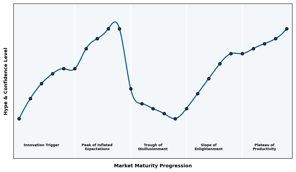
How AI is Transforming Silicon Wafer Engineering Practices
Implementation Framework
Evaluate existing infrastructure and skills
Create a roadmap for AI implementation
Test AI solutions on a small scale
Upskill employees for AI technologies
Continuously improve AI applications
Conduct a comprehensive assessment of current technological infrastructure and workforce capabilities to determine readiness for AI integration, ensuring alignment with Silicon Wafer Engineering goals and AI strategies for improved efficiencies.
Internal R&D
Design a strategic plan that outlines specific goals, technologies, and methodologies for AI adoption in Silicon Wafer Engineering , aligning with industry standards and addressing scalability and integration concerns for optimal performance.
Technology Partners
Initiate pilot projects to validate AI technologies within controlled environments, assessing their impact on process optimization, yield improvement, and cost reductions in Silicon Wafer Engineering , while gathering insights for broader rollout.
Industry Standards
Provide targeted training programs and workshops for employees to enhance their understanding of AI tools and methodologies, fostering a culture of innovation and ensuring successful adoption in Silicon Wafer Engineering operations and analytics.
Cloud Platform
Establish ongoing monitoring systems to assess the performance of AI implementations, making iterative adjustments based on data analytics to optimize outcomes and maintain competitive advantage in Silicon Wafer Engineering .
Internal R&D
The path to a trillion-dollar semiconductor industry by 2030 requires rethinking how manufacturers collaborate, leverage data, and deploy AI-driven automation to squeeze out 10% more capacity from factories.
– John Kibarian, CEO of PDF Solutions
Compliance Case Studies


Seize the opportunity to transform your silicon wafer engineering with AI-driven solutions. Stay ahead of the competition and unlock unparalleled efficiency and innovation today!
Take TestAdoption Challenges & Solutions
Data Silos and Fragmentation
Utilize AI Adoption Fab Case Studies to integrate disparate data sources into a unified platform. Employ advanced data analytics to provide real-time insights and facilitate cross-departmental collaboration. This approach enhances decision-making and improves operational efficiency in Silicon Wafer Engineering.
Resistance to Change
Implement AI Adoption Fab Case Studies through change management strategies that include stakeholder engagement and training. Establish pilot projects to demonstrate tangible benefits, fostering a culture of innovation. This mitigates resistance and encourages adoption across teams, ultimately enhancing productivity.
High Initial Investment
Address budget concerns by leveraging AI Adoption Fab Case Studies' modular implementation approach. Start with low-cost pilot projects that deliver quick ROI, enabling reinvestment into broader initiatives. This phased strategy minimizes financial risk while showcasing the technology's value in Silicon Wafer Engineering.
Compliance Complexity
Utilize AI Adoption Fab Case Studies to automate compliance tracking and reporting in Silicon Wafer Engineering. Integrate real-time data analytics to identify risks and ensure adherence to industry standards, streamlining audits and reducing the administrative burden of compliance management.
Assess how well your AI initiatives align with your business goals
AI Use Case vs ROI Timeline
| AI Use Case | Description | Typical ROI Timeline | Expected ROI Impact |
|---|---|---|---|
| Predictive Maintenance for Equipment | AI algorithms analyze sensor data to predict when machinery will fail, reducing downtime. For example, using machine learning to assess vibration data from wafer fabrication equipment can prevent costly breakdowns and ensure smoother operations. | 6-12 months | High |
| Quality Control Automation | AI-powered vision systems inspect wafers for defects in real time, enhancing product quality. For example, implementing image recognition technology to detect microscopic imperfections can significantly lower rejection rates and improve yield. | 6-12 months | Medium-High |
| Supply Chain Optimization | AI tools optimize inventory and supply chain logistics, reducing costs and delays. For example, using predictive analytics to forecast raw material needs for wafer production ensures a smooth supply flow and minimizes waste. | 12-18 months | Medium |
| Process Optimization in Fabrication | AI models analyze production data to optimize process parameters for wafer fabrication. For example, machine learning can identify optimal temperature settings in etching processes, enhancing efficiency and reducing resource consumption. | 6-12 months | Medium-High |
Glossary
Work with Atomic Loops to architect your AI implementation roadmap — from PoC to enterprise scale.
Contact NowFrequently Asked Questions
- Identify specific processes that can benefit from AI applications and automation.
- Engage stakeholders to ensure alignment on objectives and desired outcomes.
- Assess existing infrastructure and capabilities to facilitate integration.
- Consider piloting AI solutions in low-risk environments for initial testing.
- Gather feedback and iterate on AI applications to optimize performance.
- AI enhances productivity by automating repetitive tasks and optimizing workflows.
- Companies can achieve significant cost reductions through efficient resource management.
- Data-driven insights lead to improved decision-making and strategic planning.
- AI adoption can foster innovation, enabling faster product development cycles.
- Competitive advantages arise from enhanced quality and customer satisfaction metrics.
- Resistance to change from employees can hinder successful AI implementation efforts.
- Integration with legacy systems may pose technical challenges during deployment.
- Data quality and availability are critical for effective AI model training and application.
- Skill gaps in the workforce necessitate training and potential hiring of specialists.
- Clear communication and change management strategies can help mitigate these challenges.
- Organizations should evaluate their digital maturity before embarking on AI initiatives.
- A clear understanding of business goals will guide timing for AI adoption.
- Market conditions may create urgency for adopting AI to maintain competitiveness.
- Consider seasonal production cycles when planning AI implementation timelines.
- Ensure resources and stakeholder buy-in are in place for a successful launch.
- AI can optimize manufacturing processes through predictive maintenance and quality control.
- Data analytics enable improved yield management and defect detection.
- Machine learning algorithms assist in process adjustments to enhance efficiency.
- AI-driven simulations can forecast outcomes and optimize design parameters.
- Robotics integrated with AI can facilitate precision in handling sensitive materials.
- Compliance with industry standards ensures AI applications meet safety and quality benchmarks.
- Data privacy regulations must be adhered to when handling sensitive information.
- Transparency in AI decision-making processes can help mitigate compliance risks.
- Regular audits may be necessary to ensure ongoing adherence to regulatory requirements.
- Engaging legal experts early in the process will help navigate complex regulations.
- Establish clear success metrics that align with business objectives from the outset.
- Track operational efficiencies and cost savings attributed to AI implementations.
- Evaluate improvements in product quality and customer satisfaction over time.
- Conduct regular reviews to assess the impact of AI on overall business performance.
- Use benchmarking against industry standards to gauge competitive positioning.
- Start with a clear strategy that outlines goals, resources, and expected outcomes.
- Involve cross-functional teams to ensure diverse perspectives and expertise are included.
- Iterate and refine AI applications based on real-world performance and user feedback.
- Invest in ongoing training and support to foster a culture of continuous improvement.
- Document learnings and successes to guide future AI initiatives across the organization.